NEW DELHI — In the chess game of global technology leadership, New Delhi has just made its most aggressive opening gambit yet. On August 15, 2025, the Government of India, via its Press Information Bureau (PIB), released a comprehensive blueprint titled "Powering the Future: The Semiconductor and AI Revolution." The document signals a historic shift: India is transitioning from a consumer of global technology to a primary sovereign producer of silicon and artificial intelligence.
As Western tech giants seek "China+1" supply chain alternatives and artificial intelligence demands unprecedented compute capacity, India's dual-engine strategy—leveraging the India Semiconductor Mission (ISM) alongside the newly energized IndiaAI Mission—aims to establish the nation as a premier global hub for deep technology.
For global investors, multinational tech firms, and policymakers, the implications are clear: India is no longer just the world’s back office; it is positioning itself as the foundational engine of the next industrial revolution.
The Silicon Bedrock: Inside India's Semiconductor Super-Cycle
At the heart of India's technological leap is the India Semiconductor Mission (ISM), backed by a massive ₹76,000 crore (approximately $9.1 billion) incentive program. According to the federal factsheet, this initiative is designed to build a complete, end-to-end semiconductor ecosystem within the country. Rather than focusing solely on low-value assembly, the government's strategy spans silicon fab manufacturing, packaging, design, and testing.
The capital expenditure wave is already translating into brick-and-mortar reality. Key mega-projects approved and currently under construction include:
- Dholera (Gujarat): Tata Electronics, in partnership with Taiwan's PSMC, is constructing India’s first commercial semiconductor fab, a mega-facility with a projected capacity of up to 50,000 wafer starts per month.
- Sanand (Gujarat): Micron Technology’s advanced semiconductor testing and packaging (ATMP) facility, alongside CG Power and Renesas' joint venture packaging plant.
- Morigaon (Assam): Tata Semiconductor Assembly and Test (TSAT) is establishing an ultra-modern packaging facility, bringing high-tech manufacturing to India’s Northeast.
- Kaynes Semicon (Sanand): A newly authorized unit focused on advanced co-packaged optics and silicon assembly.
By offering up to 50% fiscal support for semiconductor fabs and packaging plants, New Delhi has successfully compressed a decade’s worth of industrial planning into less than three years, positioning the nation as a key node in the global silicon value chain.
The Intelligence Layer: Scaling Sovereign AI
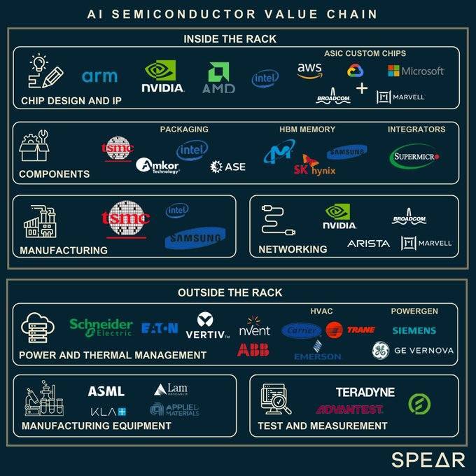
If semiconductors are the body of this new industrial architecture, Artificial Intelligence is the mind. To ensure India does not become reliant on foreign proprietary AI models, the Union Cabinet has operationalized the IndiaAI Mission with a dedicated budget of ₹10,372 crore.
Rather than leaving AI development entirely to market forces, India’s public-private partnership model focuses on building democratized, sovereign infrastructure. Key pillars of this initiative include:
1. Sovereign Compute Infrastructure
The mission is funding the procurement of over 10,000 high-performance GPUs (graphics processing units) through public-private partnerships. This compute capacity will be made available as a service to Indian startups, researchers, and public enterprises at subsidized rates, breaking the monopoly of hyper-scalers.
2. The IndiaAI Innovation Centre & Native LLMs
A specialized agency focused on developing indigenous foundational models, specifically targeting India’s 22 official languages. This ensures that AI applications are culturally, linguistically, and economically tailored to the domestic market, particularly in critical sectors like agriculture, healthcare, and digital governance.
3. FutureSkills Initiative
To feed this growing industry, the government is partnering with premier institutions (IITs, NITs) to establish specialized chip design and AI research programs, aiming to train over 100,000 highly skilled engineers within the next three years.
Comparing India’s Dual Engines: Semiconductor vs. AI
To understand the scale and focus of India’s technological roadmap, the table below highlights the comparative allocations, strategic objectives, and key milestones outlined in the latest federal framework:
| Strategic Dimension | India Semiconductor Mission (ISM) | IndiaAI Mission |
|---|---|---|
| Financial Allocation | ₹76,000 Crore (~$9.1 Billion USD) | ₹10,372 Crore (~$1.24 Billion USD) |
| Primary Objective | Build domestic hardware manufacturing, fabs, and ATMP units. | Establish sovereign AI compute, native LLMs, and ecosystem startups. |
| Key Global Partners | PSMC (Taiwan), Micron (US), Renesas (Japan) | Global AI developers, academic institutions, chip manufacturers |
| Target Milestones | Operational commercial fabs by 2026-27; domestic chip packaging hubs. | 10,000+ GPU supercomputing capacity; indigenous multi-lingual LLMs. |
| Strategic Focus Area | Hardware sovereignty and global supply chain de-risking. | Software democratization, local innovation, and talent scaling. |
Silicon Diplomacy: The Geopolitical Play
The alignment of these two missions is not just an economic strategy; it is a geopolitical masterstroke. The global semiconductor landscape is highly consolidated, with Taiwan, South Korea, and the United States holding critical monopolies. By entering agreements like the US-India Initiative on Critical and Emerging Technology (iCET) and signing memorandum agreements on semiconductor supply chains with Japan and the European Union, India is asserting itself as a trusted, democratic alternative.
This strategy addresses the growing global demand for supply chain diversification. As global boardrooms look to hedge their manufacturing bets, India’s stable regulatory environment, massive domestic consumer market, and targeted subsidies present a highly compelling proposition.
The Road Ahead: Navigating Structural Bottlenecks
Despite the immense momentum, structural challenges remain. Semiconductor fabrication is incredibly capital-intensive and demands flawless utility infrastructure. Fabs require uninterrupted, ultra-pure water supplies and a continuous, surge-free electrical grid—elements that have historically tested India's municipal infrastructure. Furthermore, while India boasts nearly 20% of the world's chip design talent, transition from design ("fabless") to physical manufacturing ("fab") requires a specialized workforce that must be scaled up rapidly.
However, with deep corporate backing from domestic conglomerates like Tata and Larsen & Toubro, alongside concrete policy support from New Delhi, India’s trajectory is clear. The convergence of silicon and intelligence marks a defining moment. India is no longer waiting for the future to arrive; it is actively manufacturing it.
Frequently Asked Questions
Why is India focusing on both Semiconductors and AI simultaneously?
Semiconductors and Artificial Intelligence are intrinsically linked; advanced AI software requires highly specialized silicon hardware (GPUs and TPUs) to run. By developing both ecosystems simultaneously, India ensures that its domestic AI developers have reliable access to high-performance hardware, while its manufacturing facilities have a guaranteed domestic customer base. This unified approach reduces external dependencies and secures technological sovereignty.
How will the IndiaAI Mission benefit local startups and developers?
The IndiaAI Mission directly addresses the high entry barriers of the AI industry by establishing public-private compute infrastructure. Startups and researchers will gain subsidized access to a network of 10,000+ GPUs, which would otherwise be cost-prohibitive. Furthermore, the development of localized, open-source Large Language Models (LLMs) in regional languages enables developers to build custom applications for domestic sectors like finance, agriculture, and healthcare.