IBM’s 0.7nm Nanostack Breakthrough Reshapes Global Semiconductor Economics and AI Infrastructure
Test Our Free AI & Tech Utilities Suite
Calculate LLM API token costs, analyze article dwell-time, or simulate tech DCA returns.
International Business Machines (IBM) has fundamentally altered the trajectory of next-generation semiconductor manufacturing and artificial intelligence compute architecture. According to verified reports originating from premier wire services, IBM is officially opening its revolutionary 0.7-nanometer (0.7nm) "Nanostack" architecture to third-party chip designers in the first quarter of 2027. This milestone involves the widespread commercial shipment of Process Design Kits (PDKs), providing fabless designers, hyperscalers, and enterprise silicon architects with the foundational toolsets required to build sub-nanometer processors.
As large language models (LLMs) and generative artificial intelligence inferencing engines strain global power grids and test the limits of physical scaling, the semiconductor industry has faced a looming wall governed by the limits of traditional planar and FinFET geometries. IBM’s 0.7nm Nanostack process introduces vertical monolithic stacking and advanced gate-all-around (GAA) optimizations designed to circumvent current thermal and spatial constraints. For institutional investors, venture capital syndicates, and corporate technology leaders, this announcement serves as a massive catalyst that will inevitably trigger a reallocation of capital expenditure across the global hardware supply chain.
Executive Takeaways
- Commercial Timeline: IBM will officially distribute its 0.7nm Nanostack Process Design Kits (PDKs) to external chip designers starting in Q1 2027.
- Architectural Leap: Moving far beyond conventional 2nm and 1.4nm roadmaps, the 0.7nm Nanostack architecture utilizes vertical integration to maximize transistor density while mitigating leakage current.
- AI Infrastructure ROI: The technology promises exponential reductions in die size, directly addressing the soaring thermal dissipation and power consumption metrics plaguing modern AI data centers.
- Market Revaluation: The move threatens to upend traditional foundry dominance by positioning IBM as a premier licensor of high-end IP, forcing rivals like TSMC, Intel, and Samsung to accelerate their own vertical integration roadmaps.
The Catalytic Shift: Overcoming the Physical Limits of Silicon Scaling
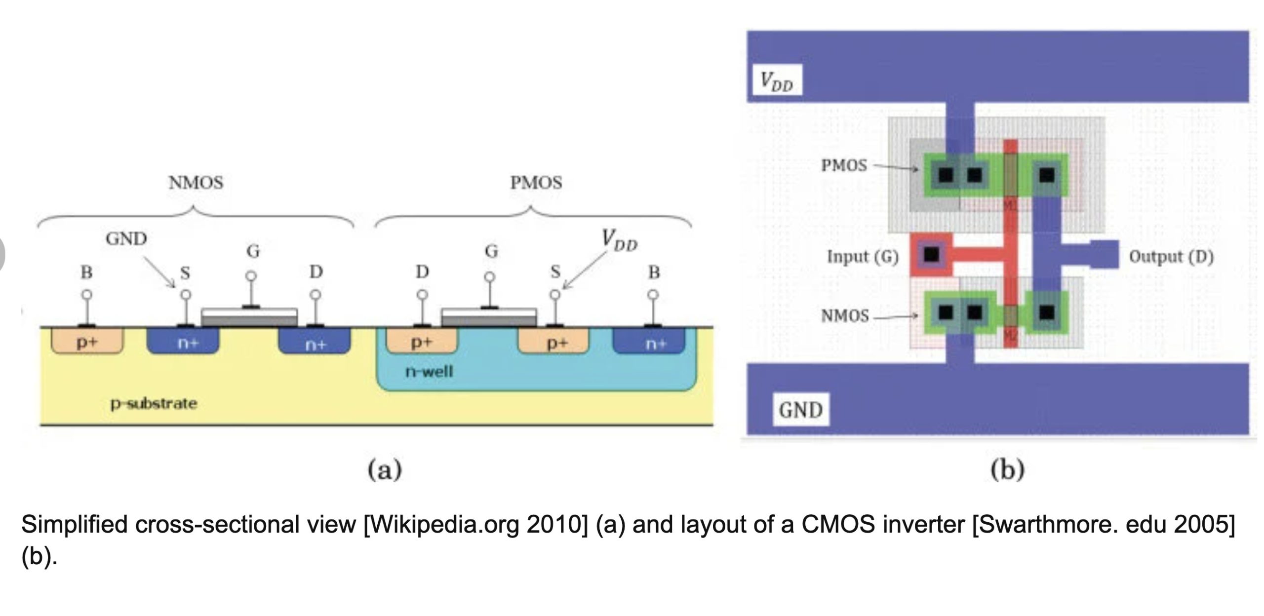
For decades, Moore’s Law governed the cadence of the semiconductor industry, dictating that the number of transistors on a microchip doubles roughly every two years. However, as the industry transitioned from 7nm down to 3nm nodes, physicists and materials scientists encountered severe quantum mechanical hurdles. Electron tunneling, extreme current leakage, and catastrophic thermal densities threatened to halt progress entirely. While industry giants pivoted toward nanosheet and Gate-All-Around (GAA) architectures, horizontal scaling alone could no longer deliver the performance-per-watt metrics demanded by modern enterprise AI workloads.
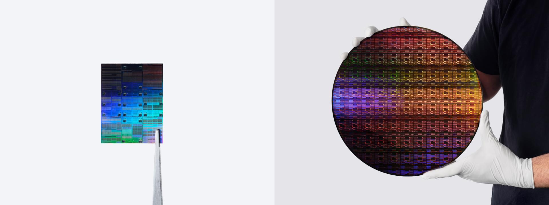
IBM’s historical pedigree in semiconductor research—marked by its invention of the original GAA transistor concept and decades of breakthrough work at the Albany Nanotech Complex—has culminated in the 0.7nm Nanostack process. Unlike standard planar or single-layer nanosheet designs, Nanostack leverages true three-dimensional monolithic integration. By vertically stacking active transistor layers on top of one another, IBM has effectively bypassed the footprint limitations of traditional horizontal die design.
The decision to open this proprietary process via PDK distribution in Q1 2027 signals a strategic pivot from internal research to aggressive commercialization. By putting design kits into the hands of fabless semiconductor companies, IBM is democratizing access to sub-nanometer geometries. This empowers enterprise buyers to design custom Application-Specific Integrated Circuits (ASICs) tailored explicitly for neural network training and high-performance computing (HPC) without being bottlenecked by legacy foundry limitations.
Financial, Operational, and Infrastructure Implications
The introduction of a viable 0.7nm production-ready design ecosystem carries profound financial and operational implications across global markets. From an enterprise risk mitigation perspective, relying on a consolidated geographic supply chain for advanced AI accelerators has long troubled Chief Information Officers (CIOs) and corporate boardrooms. IBM’s licensing and PDK strategy diversifies the technological pipeline, offering a vital competitive counterweight in an industry prone to geopolitical friction and supply chain bottlenecks.
Capital Allocation and Valuation Multiples
Hyperscale cloud service providers—including Microsoft, Amazon Web Services, Google Cloud, and Meta—spend tens of billions of dollars annually on custom AI silicon. However, the physical footprint and power envelopes of current accelerators have reached a breaking point, driving up capital expenditure (CapEx) and compressing operating margins. By shrinking die sizes down to the 0.7nm threshold through Nanostack technology, chip designers can dramatically increase wafer yield efficiency. Higher yields translate directly into lower per-unit manufacturing costs, bolstering enterprise ROI and stabilizing valuation multiples for hardware-dependent software enterprises.
Cloud Compute Architecture and Power Efficiency
Data center operators face an impending power crisis. Modern AI training clusters require megawatts of continuous energy, straining municipal power grids and forcing operators to explore dedicated nuclear or renewable energy microgrids. IBM’s 0.7nm Nanostack process directly attacks this inefficiency by reducing parasitic capacitance and operating voltages. Lower operational voltages reduce thermal output, subsequently slashing the auxiliary power required for liquid and air-cooling infrastructure within hyperscale facilities.
Verified Data and Specifications Breakdown
To contextualize the technological leap represented by IBM’s announcement, the following comparative matrix outlines the projected specifications and operational milestones of the 0.7nm Nanostack process against prevailing industry standards.
| Parameter / Metric | Standard 3nm / 2nm FinFET/GAA | IBM 0.7nm Nanostack Process | Commercial Impact |
|---|---|---|---|
| PDK Availability Date | Currently Available (2023–2025) | Q1 2027 | Sets the timeline for next-gen fabless development cycles. |
| Transistor Architecture | Horizontal Nanosheet / GAA | Monolithic Vertical 3D Nanostack | Doubles functional density per square millimeter. |
| Power Efficiency Gain | Baseline (1x) | Estimated 40%–50% Reduction | Mitigates data center cooling crises and power grid strain. |
| Primary Target Market | Consumer Mobile & Standard AI | Hyperscale AI Accelerators & HPC | Directly targets LLM training and complex generative workloads. |
Frequently Asked Questions (People Also Ask)
What is IBM’s 0.7nm Nanostack process?
IBM’s 0.7nm Nanostack is an advanced semiconductor fabrication architecture that utilizes monolithic vertical stacking of transistors. By moving beyond traditional horizontal scaling and embracing true 3D integration at sub-nanometer geometries, it drastically increases transistor density while managing current leakage and thermal output.
When will chip designers gain access to IBM’s 0.7nm technology?
IBM has scheduled the official distribution of its Process Design Kits (PDKs) for the 0.7nm Nanostack architecture to external chip designers in the first quarter of (Q1) 2027. This allows engineering teams to begin prototyping custom silicon well ahead of mass production runs.
How does this technology impact artificial intelligence hardware development?
As AI models grow exponentially in parameter size, traditional silicon footprints struggle with power and thermal bottlenecks. The 0.7nm Nanostack process enables significantly smaller die sizes and vastly improved energy efficiency, allowing AI accelerators to deliver higher computational throughput while consuming less electrical power.
Who are the primary beneficiaries of this semiconductor breakthrough?
The primary beneficiaries include fabless semiconductor companies, enterprise cloud hyperscalers (such as Microsoft, Google, and Amazon), and enterprise clients seeking custom AI accelerators with superior power-performance ratios. It also positions IBM strongly within the high-value intellectual property licensing and advanced research ecosystem.
Future Outlook and Strategic Milestones to Watch
As the industry counts down to the Q1 2027 PDK release, market analysts and industry insiders will monitor several critical milestones. First, strategic partnerships announcements between IBM and major foundry partners—such as Samsung, Rapidus, or Intel Foundry—will dictate how quickly these designs can transition from digital blueprints to physical silicon wafers.
Second, enterprise adoption rates among hyperscalers will serve as a bellwether for the commercial viability of monolithic 3D stacking over traditional packaging methods like chiplets and 2.5D interposers. While chiplet architectures have dominated recent packaging discussions, IBM’s Nanostack aims to offer a complementary or superior path for ultra-dense, low-latency compute cores.
Ultimately, IBM’s aggressive push into the 0.7nm tier underscores a fundamental truth of modern economic life: computational supremacy remains the ultimate currency of the digital age. For executives, investors, and technologists navigating the next decade of enterprise expansion, tracking the rollout of IBM’s Nanostack process will be essential for anticipating where the next wave of technological disruption—and financial return—will originate.