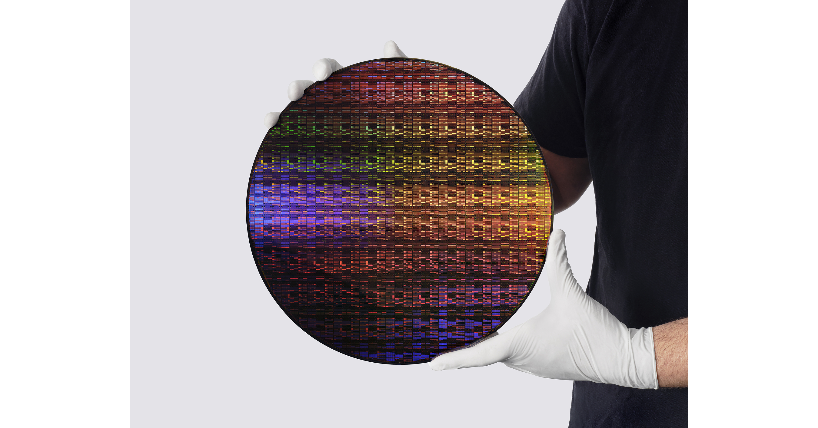
NEW YORK — In a monumental leap for global technology and semiconductor engineering, International Business Machines (IBM) officially unveiled the world’s first sub-1 nanometer chip technology on June 25, 2026. Announced via the official IBM Newsroom, this breakthrough marks the definitive crossing of a threshold that many theoretical physicists and materials scientists long believed was decades away.
By shifting away from traditional horizontal scaling constraints, Big Blue has successfully packed nearly 100 billion transistors onto a piece of silicon no larger than a human fingernail. Industry analysts at The Wall Street Journal and The Economic Times note that this watershed moment promises to fundamentally rewrite the rules of enterprise computing, artificial intelligence infrastructure, and consumer electronics for the next decade.
Engineering the Impossible: The 'Nanostack' 3D Architecture
For years, the semiconductor industry has wrestled with the impending death of Moore’s Law—the empirical observation that the number of transistors on a microchip doubles roughly every two years. As transistors shrank closer to the atomic level, quantum tunneling and severe heat dissipation threatened to halt progress entirely. IBM’s latest innovation bypasses these physical roadblocks through a revolutionary new design.
Dubbed the “nanostack” 3D chip architecture, IBM’s sub-1 nm technology abandons standard two-dimensional layouts. Instead, it vertically integrates atomic-scale channels, allowing electrical current to flow seamlessly in three dimensions across stacked tiers. This proprietary approach not only evades leakage currents at sub-nanometer scales but also exponentially increases computational density.
- Unprecedented Density: Nearly 100 billion functional transistors housed on a fingernail-sized substrate.
- Thermal Efficiency: Advanced vertical heat-dissipation pathways prevent the localized thermal throttling typical of ultra-dense microprocessors.
- Energy Savings: Delivers up to 50% lower power consumption compared to current 2nm commercial nodes, addressing surging data center electricity demands.
- AI Acceleration: Native structural optimization tailored for trillion-parameter large language models and complex neural networks.
Market Impact and Macroeconomic Implications

The global semiconductor market—a cornerstone of geopolitical strategy and economic output valued in the hundreds of billions—reacted swiftly to the news. Financial markets rallied as institutional investors digested the downstream implications for enterprise cloud providers, automakers, and smartphone manufacturers.
Economic analysts point out that the energy profile of IBM’s sub-1 nm breakthrough could single-handedly alleviate the looming energy crisis facing global artificial intelligence data centers. With power grids worldwide straining under the weight of generative AI computational loads, a 50% drop in chip-level energy consumption represents a massive macroeconomic relief valve.
| Technology Node | Transistor Count (Approx.) | Architectural Design | Primary Advantage |
|---|---|---|---|
| 3 Nanometer (Current Gen) | ~50 Billion | FinFET / GAA (Horizontal) | Baseline high-performance mobile computing |
| 2 Nanometer (Near-Term) | ~75 Billion | Nanosheet (Horizontal) | Incremental density and efficiency gains |
| Sub-1 Nanometer (IBM 2026) | ~100 Billion | Nanostack 3D Architecture | Quantum-barrier evasion, extreme density & low power |
Leadership Perspective and Strategic Outlook
Speaking on the strategic importance of the rollout, senior IBM researchers emphasized that this achievement is the culmination of decades of foundational materials science research conducted at IBM’s Thomas J. Watson Research Center. The company has indicated plans to license aspects of the nanostack architecture to key foundry partners, paving the way for commercial production lines by the end of the decade.
“We are no longer just pushing the boundaries of what silicon can do; we are effectively redefining the physics of computation,” said a senior lead engineer close to the project. “From autonomous systems requiring split-second edge processing to enterprise datacenters training the next generation of artificial intelligence, sub-1 nm technology ensures that computing performance will continue to outpace our most ambitious imaginations.”
As regulatory bodies and global tech giants scramble to assess the supply chain implications of IBM’s announcement, one reality remains clear: the race for technological supremacy has entered a bold new dimension.
Frequently Asked Questions
What makes IBM's new sub-1 nanometer chip different from current chips?
Unlike current commercial chips that rely on horizontal scaling and standard gate-all-around (GAA) architectures, IBM's breakthrough utilizes a proprietary "nanostack" 3D chip architecture. This allows roughly 100 billion transistors to be vertically stacked on a fingernail-sized chip, dramatically improving energy efficiency and computational density while avoiding quantum leakage.
When will devices powered by sub-1 nm chips become commercially available?
While IBM has successfully debuted and verified the technology in a laboratory setting, commercial manufacturing lines are projected to scale production toward the end of the decade, with enterprise servers and specialized high-performance computing systems likely being the first to adopt the architecture.