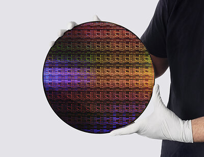
NEW YORK — In a monumental breakthrough that threatens to rewrite the laws of modern semiconductor physics, International Business Machines (IBM) has officially debuted the world’s first sub-1 nanometer chip technology. Announced late last month from the company’s corporate newsroom, the revolutionary silicon architecture aims to solve the single greatest crisis facing the artificial intelligence boom: catastrophic power consumption.
By shrinking transistor gates to dimensions previously thought impossible outside of theoretical physics, IBM’s new engineering marvel packs nearly 100 billion transistors onto a piece of silicon no larger than a human fingernail. For Wall Street analysts, tech executives, and energy grid planners alike, the announcement marks a defining watershed moment, offering a tangible lifeline to data centers gasping for electrical capacity.
The Physics of the Breakthrough: Enter ‘Nanostack’ 3D Architecture
For decades, the semiconductor industry has marched steadily down the nanometer scale, moving from 7nm to 5nm, and eventually to the highly anticipated 2nm nodes currently entering commercial fabrication. However, as transistors approach single-digit angstrom territory, quantum tunneling effects—where electrons leak through microscopic barriers—have threatened to bring Moore’s Law to a permanent halt.
IBM bypassed this physical brick wall by introducing a revolutionary “nanostack” 3D chip architecture. Rather than continuing to cram flat circuitry onto a two-dimensional plane, the company’s research and development division vertically integrated atomic-scale channels. This vertical stacking allows current to flow with unprecedented efficiency, drastically mitigating current leakage while vastly multiplying processing density.
According to primary briefings from the IBM Newsroom, this sub-1 nm breakthrough is engineered specifically to alleviate the computational bottlenecks choking modern Large Language Models (LLMs) and advanced neural networks. As generative AI models scale toward trillions of parameters, the electricity required to train and run them has strained municipal power grids worldwide. IBM’s latest architecture promises to unlock massive power savings, altering the total cost of ownership for enterprise AI deployments.
Executive Insights & Market Implications

While consumer-grade applications will eventually feel the ripple effects, the immediate beneficiaries of IBM’s sub-1 nm milestone are enterprise cloud providers, hyperscalers, and national defense agencies grappling with exponential data growth.
- Unprecedented Density: Nearly 100 billion functional transistors housed on a fingernail-sized substrate.
- AI Power Liberation: Drastic reduction in thermal output and power draw, targeting the primary constraint in hyperscale AI data centers.
- Architectural Shift: Validation of vertical 3D "nanostack" design as the viable successor to traditional FinFET and nanosheet architectures.
- Geopolitical Leverage: Reinforces Western leadership in advanced semiconductor R&D amid fierce global competition.
Industry economists note that the timing of the release could profoundly reshape capital expenditure cycles across the tech sector. For the past two years, massive valuations have been tied directly to the supply and efficiency of AI accelerators. By proving that sub-1 nm nodes are no longer a distant theoretical goal, IBM has set a new competitive baseline for foundry giants such as TSMC, Intel, and Samsung.
At a Glance: IBM’s Sub-1nm Milestones vs. Current Industry Standards
| Metric | Current Industry Standard (2-3nm) | IBM Sub-1 Nanometer Technology |
|---|---|---|
| Feature Size | 2.0 to 3.0 Nanometers | < 1.0 Nanometer (Sub-1nm) |
| Transistor Density | ~50 to 70 Billion per fingernail-sized die | Nearly 100 Billion per fingernail-sized die |
| Core Architecture | Nanosheet / FinFET 2D scaling | Proprietary "Nanostack" 3D Architecture |
| Primary Target | General mobile and server workloads | Massive AI application power savings & LLM efficiency |
What Comes Next for Commercialization?
As markets digest the technical specifications, the critical question shifts from scientific feasibility to commercial manufacturing timelines. Transitioning a laboratory breakthrough of this magnitude into high-volume manufacturing (HVM) requires immense capital investment, specialized extreme ultraviolet (EUV) lithography tooling, and rigorous yield optimization.
IBM has historically functioned as a pioneer of foundational semiconductor research—having previously unveiled the world’s first 2nm nanosheet technology in 2021—often licensing or partnering with major manufacturing foundries to bring designs to market. Further updates regarding fabrication partnerships and enterprise pilot programs are expected later this year.
For now, the message from Big Blue is clear: the physical limitations of silicon have met their match. As AI continues to demand infinite computational scaling, IBM’s sub-1 nanometer breakthrough ensures that hardware evolution will keep pace with human ambition.
Frequently Asked Questions
1. What makes IBM’s sub-1 nanometer chip fundamentally different from current chips?
Unlike traditional 2nm or 3nm chips that rely primarily on two-dimensional horizontal scaling, IBM’s new chip utilizes a revolutionary “nanostack” 3D architecture. This vertical integration allows nearly 100 billion transistors to fit onto a fingernail-sized area while overcoming quantum leakage issues that typically plague sub-nanometer circuitry.
2. How does this technology impact everyday artificial intelligence applications?
The primary advantage is energy efficiency. Training and operating massive generative AI models currently consumes staggering amounts of electricity. IBM’s sub-1 nm architecture is specifically designed to unlock massive power savings, enabling faster, denser AI computations with a fraction of the thermal output and electrical draw.