By The Investigative Desk | Special Report for Konsulteer
Executive Takeaways
- Historical Foundations: India’s semiconductor ambitions are not a recent pivot; they began with the state-backed Semi-Conductor Laboratory (SCL) in Mohali, established in the 1980s.
- Capital Allocation Shift: Backed by a $10 billion federal incentive package (ISM), India is shifting from a pure software powerhouse to an integrated hardware and fabrication hub.
- Ecosystem Maturation: Current mega-investments by Tata, Micron, and CG Power are mitigating supply chain vulnerabilities, creating high-margin enterprise ROI, and attracting tier-1 global tooling vendors.
- Strategic Risk Mitigation: Geopolitical realignments and the global push for supply chain diversification are accelerating India's integration into advanced packaging and legacy node manufacturing.
For decades, global technology markets viewed India through a singular, highly lucrative lens: as the back-office engine of the digital economy, a titan of IT services, software architecture, and offshore engineering. Yet, beneath the veneer of code and cloud infrastructure, a quiet, multi-decade industrial drama has been unfolding. The narrative of India’s semiconductor evolution is neither an overnight policy reaction to post-pandemic supply chain shocks nor a fleeting political slogan. It is a fifty-year marathon marked by visionary state planning, devastating setbacks, bureaucratic inertia, and a relentless, high-stakes resurrection.
Today, as geopolitical fault lines fracture global supply chains and boardrooms demand rigorous risk mitigation, India’s semiconductor strategy has crossed a critical threshold. From the pioneering yet isolated efforts of the Semi-Conductor Laboratory (SCL) in Mohali to the multi-billion-dollar fabrication ecosystems rising in Gujarat and Assam, the world's most populous nation is engineering a structural pivot. This investigation examines how historical foundations, massive capital allocation, and shifting macroeconomic realities are converging to forge a formidable new player in the global silicon economy.
The Genesis: SCL Mohali and the Early Vision of Silicon Sovereignty
To understand the trajectory of modern Indian semiconductor manufacturing, one must return to the late 1970s and 1980s—an era when India’s industrial policy was defined by autarky and state-led enterprise. Recognizing that microelectronics would dictate future geopolitical and economic power, the Government of India established the Semi-Conductor Laboratory (SCL) in Mohali, Punjab, in 1983 under the auspices of the Department of Electronics.
SCL was not merely a research outpost; it was designed as an end-to-end commercial fabrication facility. Operating on 100mm (4-inch) wafers and later targeting 150mm (6-inch) capabilities at 3-micron and 0.8-micron nodes, SCL produced integrated circuits for telecommunications, watches, and strategic defense applications. However, the enterprise faced severe headwinds. Chronic capital starvation, isolation from rapid global technological iterations, and a devastating fire in 1989 that leveled its cleanroom facilities crippled its momentum for years.
Despite these structural impediments, SCL preserved institutional memory, cultivated indigenous engineering talent, and proved that complex silicon processing was technically feasible on Indian soil. While successive governments in the 1990s and 2000s hesitated to commit the staggering capital expenditure required to keep pace with Moore’s Law, the foundational DNA laid at Mohali quietly seeded the talent pool that would later populate design centers for global giants like Intel, Qualcomm, and AMD.
The Catalyst: The India Semiconductor Mission and Capital Re-Allocation
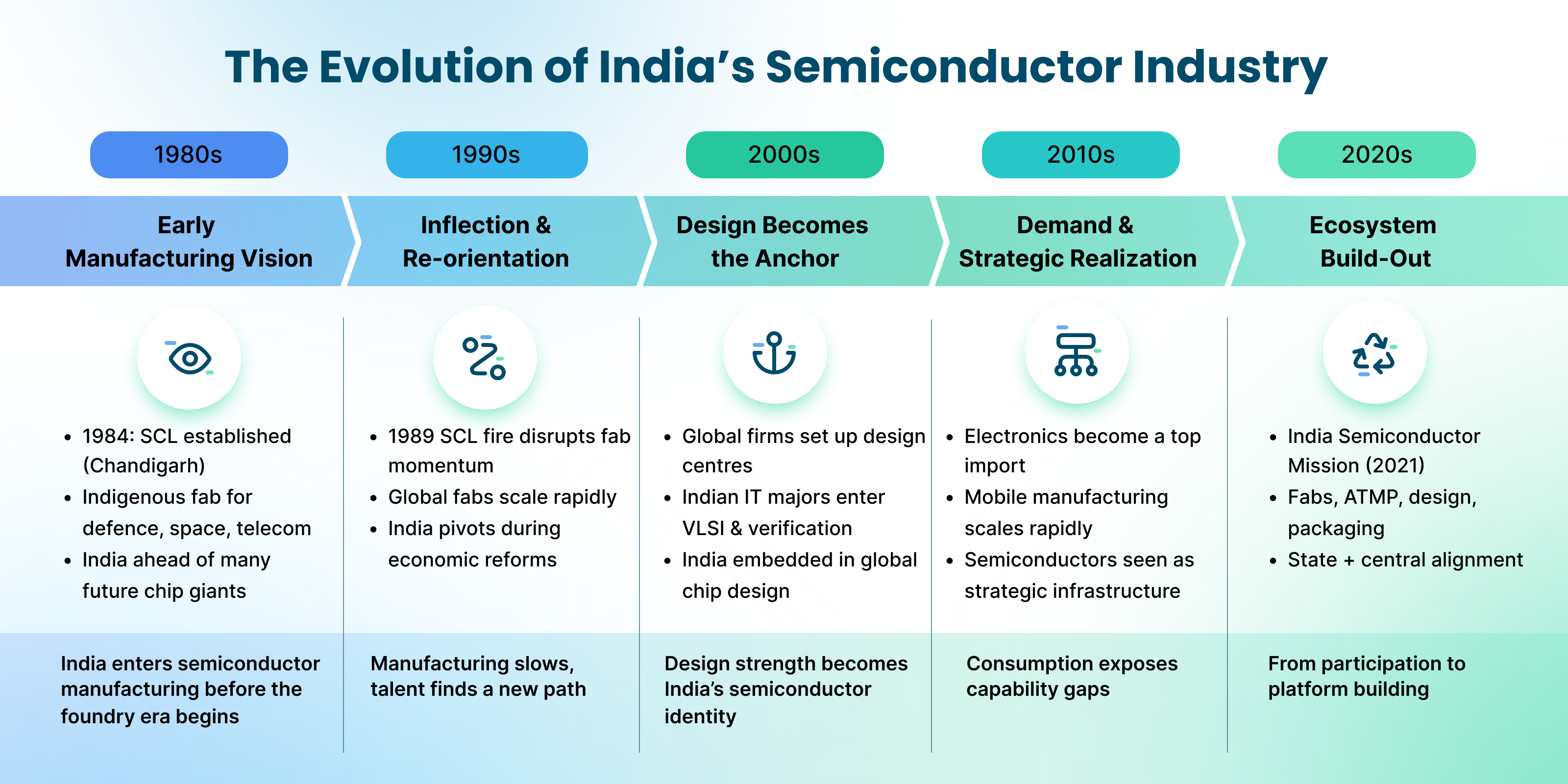
The turning point for contemporary Indian chipmaking arrived in December 2021, when the Union Cabinet approved a comprehensive $10 billion (INR 76,000 crore) incentive program known as the India Semiconductor Mission (ISM). Unlike previous policy frameworks that offered marginal tax holidays or fragmented subsidies, the ISM introduced a paradigm-shifting capital allocation strategy: the state agreed to co-fund up to 50% of capital expenditure (CapEx) for semiconductor fabs, display fabs, and compound semiconductor facilities.
This aggressive fiscal stimulus coincided with a historic structural shift in global enterprise strategy. Post-pandemic logistical bottlenecks, coupled with escalating US-China technological decoupling, forced multinational corporations (MNCs) to prioritize supply chain resilience and operational risk mitigation over pure cost minimization. India positioned itself as the logical "China+1" alternative, offering a vast domestic consumer base, competitive labor arbitrage, and robust intellectual property protections.
The financial mechanics of the ISM compelled global executives to reassess their valuation multiples regarding Indian operations. By de-risking early-stage CapEx, the Indian government effectively reduced the hurdle rate for major industrial conglomerates looking to diversify beyond East Asian manufacturing hubs.
From Blueprint to Silicon: The New Megaprojects Reshaping the Landscape
The current phase of India’s semiconductor renaissance is distinguished by private-sector heavyweight execution backed by state support. The ecosystem is no longer reliant solely on public-sector undertakings; it is being anchored by diversified industrial titans forging strategic joint ventures with global tier-1 technology leaders.
| Project / Entity | Location | Estimated CapEx | Technology / Focus Node | Strategic Impact |
|---|---|---|---|---|
| Tata Electronics & PSMC | Dholera, Gujarat | $11 Billion | 28nm to 45nm Logic & Power Management | India’s first commercial commercial foundry for automotive and consumer electronics. |
| Micron Technology | Sanand, Gujarat | $2.75 Billion | ATMP (Assembly, Test, Marking, Packaging) | Rapid operational deployment for memory testing and advanced packaging. |
| Tata Semiconductor Assembly (TSAT) | Morigaon, Assam | $3.25 Billion | Advanced Packaging, Flip Chip, and 3IC | Geographic diversification into India’s Northeast; critical for heterogeneous integration. |
| CG Power, Renesas & Stars Microelectronics | Sanand, Gujarat | $918 Million | OSAT (Outsourced Semiconductor Assembly and Test) | Strengthens legacy node packaging for industrial and automotive sectors. |
The centerpiece of this industrial expansion is the Tata Group's alliance with Taiwan’s Powerchip Semiconductor Manufacturing Corporation (PSMC) in Dholera. By targeting mature and specialty nodes (28nm to 45nm), Tata is capturing the highest-volume sweet spot of the global semiconductor market. While cutting-edge sub-3nm nodes command headlines, the vast majority of automotive systems, Internet of Things (IoT) devices, power grids, and medical instruments rely on mature nodes. By securing this foundational layer, India is anchoring itself directly into global industrial supply chains.
Simultaneously, Micron’s greenfield memory packaging facility in Sanand demonstrates the speed at which global capital can deploy when regulatory friction is minimized. Breaking ground and progressing toward commercial production within record timelines, Micron’s facility proves that India can successfully execute complex, high-precision engineering projects on par with established East Asian manufacturing hubs.
Industry & Market Implications: Winners, Losers, and Economic Re-Engineering
The maturation of India's semiconductor ecosystem carries profound macroeconomic and industrial repercussions:
- The Winners: Domestic industrial conglomerates capable of executing mega-projects (such as Tata and CG Power) stand to capture substantial market share. Global toolmakers (Applied Materials, Lam Research, ASML) find a rapidly expanding addressable market for lithography, deposition, and etch equipment. Furthermore, Indian engineering talent operating in electronic design automation (EDA) and VLSI design experience compressed career ladders and surging compensation valuations.
- The Losers: Traditional regional manufacturing hubs in East Asia face mounting competitive pressure as global firms institutionalize dual-sourcing strategies. Additionally, legacy Indian industries dependent entirely on imported electronic components must adapt or risk margin compression as local ecosystems drive domestic substitution.
- Economic Re-Engineering: The transition from an import-dependent consumer of electronics to an exporter of manufactured silicon profoundly alters India’s current account deficit. It stimulates ancillary clusters—spanning specialty chemical suppliers, ultra-pure water treatment specialists, and industrial gas providers—creating a self-sustaining industrial multiplier effect.
Frequently Asked Questions (People Also Ask)
Why did India’s early semiconductor efforts, such as SCL Mohali, fail to scale globally?
SCL Mohali suffered from a combination of chronic underfunding, technological isolation due to historical export controls (such as the Wassenaar Arrangement restrictions during the Cold War), and a catastrophic 1989 fire that destroyed its production lines. Furthermore, India’s domestic market demand at the time was insufficient to support the immense capital expenditure required to keep pace with rapid global node shrinks.
What is the India Semiconductor Mission (ISM) and how does it incentivize investors?
Launched in 2021 with a $10 billion fiscal outlay, the ISM is a specialized division within Digital India Corporation that acts as the nodal agency for implementing semiconductor policies. It provides financial support of up to 50% of project cost for semiconductor fabs, display fabs, and packaging facilities, significantly de-risking capital allocation and accelerating enterprise ROI for global joint ventures.
Why is India focusing heavily on mature nodes (28nm and above) instead of sub-3nm chips?
While sub-3nm chips dominate consumer smartphone processors, mature nodes (28nm, 40nm, 65nm, and above) represent the operational backbone of the global economy. They are essential for automotive microcontrollers, power management integrated circuits (PMICs), IoT devices, medical electronics, and defense systems. Focusing on mature nodes allows India to capture massive volume markets, build foundational engineering expertise, and establish sustainable manufacturing supply chains before attempting bleeding-edge fabrication.
How are packaging facilities (OSAT/ATMP) complementing foundry investments in India?
Advanced packaging (such as OSAT and ATMP facilities by Micron and Tata) bridges the gap between raw silicon fabrication and final system integration. As Moore's Law slows down, heterogeneous integration and advanced packaging have become critical for enhancing chip performance, thermal efficiency, and miniaturization. Establishing robust packaging capabilities ensures that India is involved in the high-value-add finishing stages of the semiconductor value chain.
Future Outlook: Milestones and Strategic Imperatives
As India transitions from political aspiration to industrial execution, the coming 36 to 60 months will serve as the ultimate stress test for the nation's semiconductor ecosystem. Success will not be measured by groundbreaking ceremonies or memoranda of understanding, but by hard operational metrics: wafer yield rates, fab uptime, environmental compliance, and the seamless integration of local component suppliers.
Key milestones to monitor include the operationalization and first commercial tape-outs from the Dholera and Sanand fabs, the successful scaling of domestic talent pipelines through specialized university-industry partnerships, and the securing of long-term offtake agreements with global fabless design houses. If India successfully navigates these operational hurdles, it will effectively rewrite the map of global hardware manufacturing—transforming half a century of foundational ambition into enduring silicon sovereignty.