The Sub-2nm Imperative: Inside the $68B Race to Redefine Silicon Supremacy, Enterprise Compute, and the Limits of Physics
Executive Takeaways
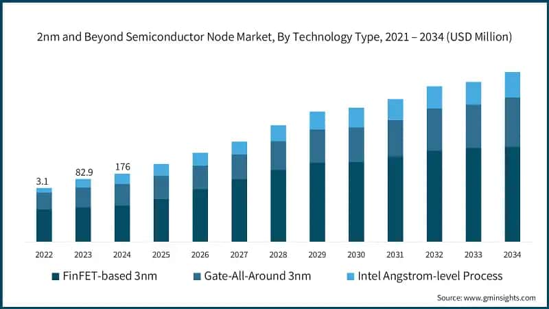
- Explosive Secular Expansion: The global 2nm and beyond semiconductor node market, benchmarked at $19.1 billion in 2024, is projected to breach $68.4 billion by 2034, compounding at a sustained 13.6% CAGR as hyperscalers re-architect global data infrastructure for monolithic AI training workloads.
- Architectural Inflection Point: The transition signals the decisive commercial death of the FinFET architecture, cementing Gate-All-Around (GAA) nanosheets, Complementary FET (CFET), and Backside Power Delivery Networks (BSPDN) as mandatory table stakes for sub-2nm fabrication.
- Capital Allocation Polarization: Ballooning tape-out expenses—exceeding $725 million per 2nm commercial design—are bifurcating the technology sector, concentrating leading-edge deployment among an elite cadre of cash-rich hyperscalers while pricing mid-tier fabless designers out of monolithic leading-edge silicon.
- Geopolitical & Capex Concentration: Extreme capital requirements ($380 million+ per High-NA EUV scanner) have concentrated the foundry battlefield down to a triad: TSMC, Intel Foundry Services (IFS), and Samsung Electronics, turning the sub-2nm roadmap into a proxy war for technological sovereignty across Washington, Brussels, and East Asia.
The Atomic Frontier: Why 2nm Breaks the Classical Scaling Playbook

For more than half a century, the semiconductor industry treated Moore’s Law not merely as an empirical observation, but as an enforceable economic contract. Today, that contract has been renegotiated at the sub-atomic scale. As revealed by market intelligence from Global Market Insights Inc., the global 2nm and beyond node market was valued at an unprecedented $19.1 billion in 2024 and is on track to advance at a compound annual growth rate (CAGR) exceeding 13.6% through 2034.
Behind this macroeconomic trajectory lies an unforgiving engineering reality: standard scaling metrics have hit the boundaries of solid-state physics. At dimensions below 20 angstroms (2 nanometers), quantum tunneling compromises classical gate oxide isolation, causing parasitic leakage currents that render legacy FinFET (Fin Field-Effect Transistor) geometries thermally unviable. The industry’s multi-billion-dollar pivot to Gate-All-Around (GAA) nanosheets—branded as RibbonFET by Intel and Multi-Bridge Channel FET (MBCFET) by Samsung—is no mere iterative refinement. It represents a ground-up reinvention of how electrostatics, materials science, and lithography converge.
To sustain power-performance-area (PPA) improvements, foundries are abandoning front-side power distribution altogether. In sub-2nm process designs, the introduction of Backside Power Delivery Networks (BSPDN)—such as Intel’s PowerVia and TSMC’s Super Power Rail—physically decouples the power rail interconnects from the signal transmission wiring. By routing current through the silicon substrate via through-silicon vias (TSVs), chip designers eliminate critical interconnect bottlenecks (RC delay), reclaim up to 20% of standard cell area, and deliver an estimated 15% to 25% surge in operating energy efficiency.
The Capex Chasm: High-NA EUV and the $700 Million Tape-Out
The transition toward 2nm and angstrom-era manufacturing has structurally disrupted the unit economics of advanced foundries. Central to this capex surge is the adoption of High-Numerical Aperture Extreme Ultraviolet (High-NA EUV) lithography. Pioneered by ASML with its Twinscan EXE:5000 and EXE:5200 systems, these 0.55 NA systems carry a per-unit capital outlay north of $380 million, requiring colossal cleanroom retrofits and dramatically altered optical path architectures.
Whereas 3nm processing relied on complex 0.33 NA EUV double-patterning techniques that bloated mask counts and suppressed wafer yields, High-NA EUV delivers 8nm half-pitch resolution in a single exposure. However, the economic barrier to entry has never been steeper. The cost of generating a single commercial tape-out at the 2nm baseline now routinely crosses $725 million when factoring in reticle development, physical design verification, EDA licensing, and yield-learning cycles. For subsequent angstrom nodes (14A and 10A), that figure is modeled to approach $1.1 billion.
Consequently, capital allocation models among fabless firms are splitting down the middle. Sovereign-scale compute buyers and multi-trillion-dollar hyperscalers (Apple, Microsoft, Alphabet, Nvidia, and Meta) possess the balance sheet liquidity to absorb these initial non-recurring engineering (NRE) expenditures. In contrast, second-tier fabless semiconductor companies are shifting toward heterogeneous chiplet architectures—combining 2nm compute dies with cost-optimized 5nm, 7nm, or mature I/O chiplets interconnected via standard Universal Chiplet Interconnect Express (UCIe) protocols.
Comparative Roadmap: The Race Across the Sub-2nm Frontier
The progression from mature 3nm nodes toward 1nm monolithic mass production has established a high-stakes competitive landscape between TSMC, Intel, and Samsung. The following table reflects the verified engineering, timeline, and cost dynamics governing the market through 2034.
| Node Classification | Commercial Target | Primary Transistor Architecture | Lithography Technology | Estimated Wafer ASP (USD) | Strategic Market Drivers |
|---|---|---|---|---|---|
| 3nm Class (N3P / SF3) | 2023–2024 | Advanced FinFET / Early GAA (Samsung) | Standard Low-NA EUV (0.33 NA) Multi-Patterning | $18,000 – $20,000 | Premium Mobile SoCs, 1st Gen AI Accelerators |
| 2nm Class (N2 / 18A / SF2) | 2025–2026 | GAA Nanosheet + Early Backside Power (BSPDN) | Low-NA EUV Double-Patterning & Early High-NA | $28,000 – $32,000 | Hyperscale LLM Inference, Advanced Enterprise HPC |
| 1.4nm Class (A14 / 14A) | 2027–2029 | Refined GAA Nanosheet / 2D Material Transistors | High-NA EUV (0.55 NA) Production Baseline | $38,000 – $44,000 | Frontier AI Training Clusters, Autonomous Defense Compute |
| 1nm & Beyond (Sub-10Å / CFET) | 2030–2034 | Complementary FET (Stacked 3D nFET/pFET) | Hyper-NA EUV (>0.75 NA) / Directed Self-Assembly (DSA) | $50,000+ | Quantum-Classical Hybrids, Post-Transformer AI Models |
Industry & Market Implications: Enterprise ROI and Geopolitical Stakes
The Geopolitical Realignment
The commercialization of the sub-2nm node is directly entangled with global industrial policy. The US CHIPS and Science Act, along with its European counterpart, were structured precisely to avoid a critical geographic choke point at the leading edge. Intel’s aggressive operational push toward its 18A and 14A nodes serves as the technological pillar for Western semiconductor reshoring. Concurrently, TSMC’s multi-billion-dollar investments in Arizona, Kumamoto, and Dresden confirm that while foundational R&D remains centered in Hsinchu and Tainan, advanced capacity is distributing geographically to de-risk supply chain exposures against East Asian geopolitical volatility.
Enterprise ROI and Cloud Compute Economics
For enterprise cloud infrastructure, the business case for adopting 2nm silicon is anchored to power budgets, cooling overhead, and total cost of ownership (TCO). In contemporary tier-4 data centers, energy procurement has eclipsed hardware acquisition as the single largest operational expense. A 2nm processor delivering a 30% reduction in power consumption at equivalent performance metrics fundamentally alters data center density. Hyperscalers can scale their FLOPs-per-megawatt envelope without running into municipal utility constraints, generating massive enterprise ROI that justifies the steep $30,000-per-wafer blended procurement cost.
Winners and Losers in the Ecosystem
- Clear Beneficiaries: Pure-play equipment monopolies (ASML, Applied Materials, Lam Research, KLA) maintain immense pricing power through proprietary intellectual property. EDA vendors (Synopsys, Cadence) benefit from a structural wave of software upgrades as designers adapt to non-planar 3D layout complexities.
- Vulnerable Players: Tier-2 foundries lacking the cash flow to finance High-NA tool acquisitions risk being permanently relegated to specialty or lagging-edge markets. Similarly, mid-sized fabless startups that lack hyperscaler-tier capital allocation reserves face existential valuation pressures if their architectural roadmaps fall an entire performance node behind.
Frequently Asked Questions (People Also Ask)
What is the core difference between 3nm and 2nm semiconductor architectures?
The primary architectural differentiator is the structural shift from FinFET to Gate-All-Around (GAA) nanosheets, combined with the integration of Backside Power Delivery Networks (BSPDN). While 3nm nodes stretched the limits of FinFETs by wrapping the gate around three sides of a vertical channel, 2nm architectures enclose the channel entirely with horizontally stacked nanosheets. This design drastically reduces subthreshold leakage, optimizes drive currents, and prevents current bleed at near-atomic scales.
Why are 2nm wafer costs estimated to exceed $30,000?
The jump in wafer ASPs reflects both the capital intensity of fabrication equipment and extreme manufacturing complexity. Generating sub-2nm features requires High-NA EUV scanners costing over $380 million each, hundreds of additional atomic layer deposition (ALD) and chemical vapor deposition (CVD) steps, specialized pellicles, and extensive defect inspection tools. Foundries must amortize these monumental multi-billion-dollar R&D and cleanroom capex investments across the initial production batches, driving up costs for early adopters.
How does Backside Power Delivery (BSPDN) improve chip efficiency?
In standard chips, both power lines and data signals are routed across the front surface, competing for limited wiring space in a complex 15-to-20-layer metal stack. This causes signal degradation, electromigration, and severe electrical resistance (IR drop). BSPDN moves the entire power supply network to the reverse side of the silicon wafer. This separates power from signal lines, lowers electrical resistance, boosts data routing density, and improves overall power efficiency by up to 20%.
Can advanced packaging replace the need for sub-2nm nodes?
Advanced packaging (such as 2.5D/3D chiplet stacking, TSMC’s CoWoS, and Intel’s Foveros) serves as a complementary approach rather than a full replacement. While packaging lets designers combine modular chiplets fabricated at different process nodes to optimize costs, foundational compute-heavy dies—such as the matrix-multiplication engines inside next-generation GPUs and AI NPUs—still rely on monolithic transistor shrinks to hit top-tier performance, thermal limits, and energy efficiency targets.
Future Outlook: The Angstrom Horizon (2025–2034)
As the market scales from its $19.1 billion foundation toward the $68.4 billion threshold in 2034, the next decade will be characterized by aggressive physical innovation. By 2027, the initial 2nm baseline will transition to 1.4nm (14A), with High-NA EUV reaching full-rate manufacturing maturity. Beyond 2030, the semiconductor industry will venture into the sub-1nm regime—often referred to as the angstrom era.
At these dimensions, the traditional nanosheet will yield to the Complementary FET (CFET), which stacks nFET and pFET transistors directly on top of one another to double logic density within the same cell footprint. Simultaneously, alternative materials—including two-dimensional transition metal dichalcogenides (TMDs) like molybdenum disulfide ($MoS_2$) and carbon nanotubes—will begin transitioning from university cleanrooms into commercial foundry pilot programs.
The 2nm milestone is therefore not the terminal point of silicon-based microelectronics. It marks the opening chapter of the angstrom era: a high-stakes, multi-billion-dollar domain where sovereign capital, atomic-level physics, and AI data centers converge to reshape the economics of global technological power.