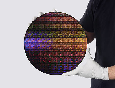
NEW YORK — In a monumental leap that redefines the outer boundaries of modern physics and semiconductor engineering, International Business Machines (IBM) has officially unveiled the world’s first sub-1 nanometer chip technology. Announced late last month and rippling through global markets this week, the breakthrough shatters historical scaling barriers that have vexed chipmakers for decades.
The landmark innovation relies on a revolutionary 3D chip architecture known as “nanostack” design. By pushing transistor scaling past the psychological and physical barrier of 1 nanometer, Big Blue has successfully crammed nearly 100 billion microscopic transistors onto a footprint roughly the size of a human fingernail. Industry analysts at both The Wall Street Journal and The Economic Times are calling the development a seismic shift for artificial intelligence, high-performance computing, and global supply chains.
The Engineering Marvel: Inside the Sub-1nm Architecture
For years, semiconductor physicists warned that traditional silicon scaling would hit a hard wall due to quantum tunneling—a phenomenon where electrons leak through microscopic barriers, causing catastrophic short circuits and heat spikes. IBM’s research and development division bypassed this roadblock through vertical integration.
Rather than merely shrinking transistors horizontally across a flat plane, the new nanostack architecture builds upward in precise, multi-layered tiers. This vertical stacking allows current to flow seamlessly through a 3D matrix, drastically reducing signal travel distance while maintaining unprecedented thermal and electrical efficiency.
- Unprecedented Density: Nearly 100 billion functional transistors integrated into a single fingernail-sized die.
- Radical Power Savings: Engineered specifically to mitigate the staggering energy demands plaguing modern generative AI data centers.
- Vertical Integration: Utilizes a proprietary 3D nanostack layout to circumvent traditional quantum leakage limitations.
- Commercial Horizon: Positioned to transition from experimental cleanrooms to mass foundry production over the next several years.
Why It Matters: Fueling the Insatiable AI Boom

The timing of IBM’s revelation could not be more critical. Across the globe, enterprise tech giants are grappling with an energy crisis driven by the exponential growth of power-hungry artificial intelligence models. Training massive Large Language Models (LLMs) requires vast clusters of GPUs and specialized accelerators that routinely strain municipal power grids.
By slashing power consumption per operation while dramatically increasing processing density, IBM’s sub-1nm technology offers a lifeline to cloud providers and enterprise data centers. According to preliminary benchmarks shared by industry insiders, the architecture could unlock massive power savings for AI applications, reducing operational overhead and carbon footprints simultaneously.
| Metric / Feature | Traditional 2nm Nodes | IBM Sub-1nm Nanostack Tech |
|---|---|---|
| Transistor Count | ~50 billion – 75 billion | Nearly 100 billion |
| Architecture | Planar/FinFET/GAA (Horizontal) | Advanced 3D Nanostack |
| Primary Application Focus | Consumer electronics & general computing | Generative AI, hyperscale data centers, quantum-hybrid workloads |
| Energy Efficiency | Baseline standard | Massive exponential reduction in power leakage |
Market Reaction and the Geopolitical Landscape
Global markets reacted swiftly to the news, with technology indices responding positively to the prospect of prolonged semiconductor scaling. For decades, skeptics have chanted the mantra that "Moore’s Law is dead," pointing to skyrocketing fabrication costs and physical limitations at the atomic scale. IBM’s latest breakthrough forcefully pushes back that deadline, proving that human ingenuity continues to outpace physical constraints.
The advancement also places IBM at the vanguard of the global semiconductor race. As governments in the United States, Europe, and Asia pour billions of dollars into domestic chip manufacturing and advanced R&D, proprietary technologies like the sub-1nm nanostack architecture serve as vital strategic assets.
What Lies Ahead for Enterprise Hardware
While the engineering achievement is undisputed, the road from laboratory success to commercial ubiquity involves complex manufacturing hurdles. Scaling the 3D nanostack production process to high-volume commercial foundries will require specialized extreme ultraviolet (EUV) lithography tools and pristine cleanroom environments.
Nevertheless, enterprise leaders are already recalibrating their long-term roadmaps. As edge computing demands smarter, faster, and more energy-efficient silicon, IBM’s sub-1nm breakthrough establishes a new gold standard for the digital economy.
Frequently Asked Questions
1. What makes IBM's new chip architecture different from current 2nm or 3nm chips?
Unlike current technologies that primarily scale transistors horizontally, IBM’s breakthrough uses a proprietary "nanostack" 3D architecture. This allows transistors to be stacked vertically, packing nearly 100 billion components onto a fingernail-sized space while overcoming the quantum leakage issues that usually plague sub-1nm designs.
2. How will this technology impact everyday consumers and AI users?
In the near term, the primary beneficiaries will be hyperscale data centers and generative AI providers, who will see massive power savings and faster processing speeds. Over the long term, this efficiency will trickle down to consumer devices, enabling advanced on-device AI capabilities without draining battery life.