Executive Takeaways
- Breaking the Physical Floor: IBM’s newly unveiled sub-1nm 3D architecture bypasses conventional lithography bottlenecks, fundamentally altering enterprise compute density.
- Vertical Integration Economics: The "Block of Flats" vertical transistor design drastically reduces enterprise capital expenditure (CapEx) per floating-point operation, threatening legacy foundry roadmaps.
- Valuation & Market Liquidity Shift: Semiconductor equities face immediate capital reallocation as institutional portfolios price in the obsolescence of planar and early 2D gate-all-around (GAA) designs.
- Geopolitical & Supply Chain Mitigation: Advanced packaging efficiencies reduce reliance on extreme ultraviolet (EUV) lithography scaling, altering sovereign trade dynamics and semiconductor fabrication plant (fab) construction costs.
NEW YORK & ZURICH — In what is rapidly being categorized by industry analysts as the most consequential hardware breakthrough of the decade, IBM has officially pierced the sub-1nm semiconductor barrier. Unveiled on June 25, 2026, the breakthrough centers on a radical 3D vertical architecture colloquially dubbed the "Block of Flats" design. By stacking functional transistor layers vertically rather than packing them laterally across a silicon wafer, IBM’s research and development division has achieved what theoretical physicists long feared was an insurmountable quantum wall: stable, commercially scalable sub-nanometer logic gates operating at room temperature with minimal quantum tunneling leakage.
For institutional investors, sovereign wealth funds, and enterprise Chief Information Officers, this announcement marks a structural pivot point. As enterprise artificial intelligence (AI) workloads, hyperscale cloud compute architecture, and autonomous simulation models push global electrical grids to their absolute limits, compute efficiency is no longer merely a performance metric—it is the ultimate determinant of valuation multiples and corporate survival. This investigative report breaks down the mechanics of IBM’s breakthrough, analyzes the macroeconomic ripple effects across global supply chains, and evaluates the long-term impact on enterprise ROI.
The Physics of the Wall: Why the Sub-1nm Barrier Mattered
For over fifty years, the semiconductor industry marched in lockstep with Moore’s Law, doubling transistor density roughly every two years. However, as fabrication nodes shrunk past the 5nm and 3nm thresholds, the industry collided with punishing fundamental laws of quantum mechanics. At scales approaching 1 nanometer—roughly the width of four silicon atoms—electrons no longer reliably obey classical gate controls. Instead, they quantum-tunnel straight through insulating barriers, generating catastrophic current leakage, extreme thermal dissipation, and structural instability.
Prior industry attempts to sustain scaling relied on Gate-All-Around (GAA) nanosheets and backside power delivery networks. While these techniques extended the life of traditional 2D lithography, they faced severe economic and physical diminishing returns. The capital expenditure required to procure high-numerical aperture (High-NA) EUV lithography systems spiraled past $400 million per unit, creating massive barrier-to-entry walls for independent foundries and squeezing operating margins.
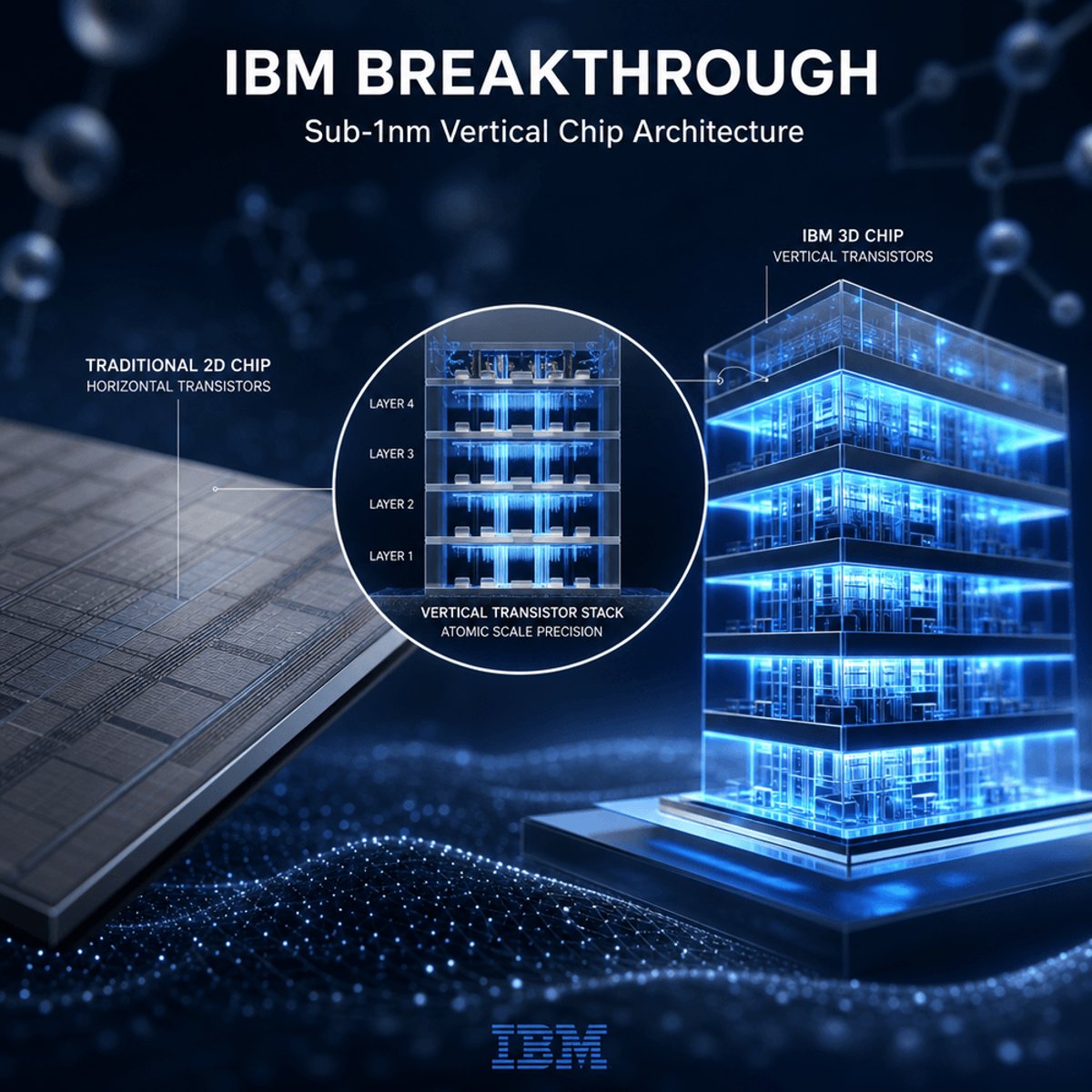
IBM’s "Block of Flats" design circumvents this physical impasse entirely. Rather than attempting to cram more circuits into a shrinking two-dimensional footprint, IBM engineers engineered a multi-tiered vertical stack. By routing power and data channels through vertical vias that mimic the structural efficiency of high-rise urban planning, the architecture isolates quantum interference while maximizing carrier mobility. The result is a dramatic reduction in parasitic capacitance and an unprecedented leap in energy efficiency.
Decoding the "Block of Flats" Architecture

To understand the enterprise implications of IBM’s June 2026 announcement, one must examine the micro-architecture. The "Block of Flats" nomenclature derives from its structural likeness to multi-story residential buildings, where independent living units share common vertical plumbing, electrical risers, and foundational support.
In traditional chip design, transistors sit side-by-side on a single plane, requiring complex, winding horizontal interconnects that introduce resistance and signal delay (RC delay). IBM’s vertical monolithic stacking places logic layers directly on top of memory and power distribution planes. This vertical co-location slashes signal travel distances by up to 70%, directly translating to lower latency and drastically reduced thermal output.
Furthermore, IBM utilized proprietary atomic-layer deposition (ALD) techniques to introduce novel high-k dielectric materials that suppress electron leakage at sub-1nm dimensions. This ensures that even under maximum enterprise compute loads—such as real-time large language model (LLM) training and petabyte-scale database queries—the silicon maintains structural integrity without requiring cryogenic cooling solutions.
Verified Data & Metrics Breakdown
A comparative analysis of historical nodes versus IBM’s sub-1nm 3D architecture highlights the scale of the engineering leap:
| Metric / Specification | Standard 3nm FinFET / GAA | IBM Sub-1nm "Block of Flats" (2026) | Enterprise Impact |
|---|---|---|---|
| Transistor Density Scaling | Baseline (1x) | 3.8x to 4.5x increase | Drastic footprint reduction per server rack. |
| Dynamic Power Consumption | High thermal envelope under load | ~55% reduction | Lowers data center cooling CapEx and operational OpEx. |
| Signal Propagation Latency | Standard horizontal RC delay | 70% reduction via vertical vias | Accelerates algorithmic execution for financial high-frequency trading and AI inference. |
| Dependence on High-NA EUV | Absolute requirement | Mitigated (relies on advanced vertical stacking) | Lowers fab construction costs and supply chain concentration risk. |
Industry & Market Implications: Winners, Losers, and Capital Allocation
Technological breakthroughs of this magnitude trigger immediate structural realignments across global financial markets. The commercialization of the sub-1nm 3D design alters competitive moats across the semiconductor ecosystem.
The Winners
- Hyperscale Cloud Providers: Companies operating massive server farms stand to realize immediate infrastructure scalability gains. By packing nearly quadruple the compute power into existing server rack footprints, capital allocation for new data center real estate can be deferred or optimized.
- Enterprise Software & AI Infrastructure: Firms specializing in generative AI, neural network training, and complex financial modeling will experience unprecedented acceleration in compute throughput, compressing training cycles from weeks to days.
- Advanced Packaging Equipment Makers: Because the "Block of Flats" architecture relies heavily on advanced vertical integration and hybrid bonding, toolmakers specializing in wafer-to-wafer stacking will capture surging enterprise procurement budgets.
The Losers & Vulnerable Segments
- Legacy Planar & Traditional Foundry Roadmaps: Foundries heavily reliant on incremental 2D scaling milestones face sudden depreciation risks on unamortized tool investments.
- High-Cost Monolithic Manufacturers: Companies unable to pivot quickly to 3D vertical monolithics risk margin compression as enterprise clients demand the superior energy efficiency and cost-per-transistor metrics inherent in IBM’s design.
Frequently Asked Questions (People Also Ask)
What does "sub-1nm" mean in practical chip manufacturing terms?
Sub-1nm refers to a node where the critical dimensions of the transistor gates and channel lengths measure under 1 nanometer. At this scale, traditional planar manufacturing fails due to quantum tunneling. IBM’s design overcomes this by moving away from horizontal scaling into a 3-dimensional vertical configuration.
How does the "Block of Flats" design reduce power consumption?
By stacking active transistor tiers vertically, electrical signals travel significantly shorter distances between logic and memory layers. This drastically lowers resistive electrical loss (RC delay) and thermal dissipation, resulting in up to a 55% reduction in dynamic power consumption compared to conventional 3nm designs.
When will enterprise data centers see commercial hardware utilizing this architecture?
Following the June 2026 technical disclosure, industry validation and pilot manufacturing runs are slated to scale over the next 18 to 24 months. Enterprise-grade server implementations and cloud deployment integrations are projected to enter commercial supply chains by late 2027 to 2028.
Does this breakthrough eliminate the need for extreme ultraviolet (EUV) lithography?
It does not completely eliminate EUV, but it significantly mitigates the industry's reliance on increasingly expensive High-NA EUV machines. By achieving density gains through vertical stacking rather than extreme lateral shrinkage, manufacturers can achieve superior performance without scaling up every single lithographic layer to its absolute physical limit.
Future Outlook & Key Milestones to Watch
As the market digests the full scope of IBM’s June 2026 revelation, financial analysts and industry observers must monitor several critical inflection points over the coming quarters:
- Foundry Licensing & Partnerships: Watch for strategic manufacturing agreements between IBM and major global foundries to transition the "Block of Flats" architecture from research labs to high-volume commercial production lines.
- Thermal Stress & Reliability Audits: Independent enterprise benchmarking regarding long-term thermal dissipation and electromigration resilience under continuous multi-terawatt AI workloads will dictate enterprise adoption speed.
- Regulatory & Export Control Adjustments: Given the profound national security and economic implications of sub-1nm compute dominance, expect regulatory bodies to evaluate how vertical 3D architectures intersect with existing semiconductor trade restrictions and export controls.
Ultimately, IBM’s sub-1nm 3D breakthrough signals the dawn of a new era in hardware engineering. By refusing to accept the physical terminality of Moore’s Law, the industry has unlocked a fresh vector of exponential growth—proving once again that human ingenuity remains the ultimate driver of market valuation and technological progress.