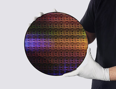
NEW YORK — In a watershed moment for global technology, International Business Machines (IBM) has officially unveiled the world’s first sub-1 nanometer semiconductor architecture. The breakthrough promises to rewrite the laws of physics that have governed computing for decades, ushering in an era of unprecedented computational density and energy efficiency.
Announced via the IBM Newsroom on June 25, 2026, the landmark development leverages a revolutionary "nanostack" 3D chip architecture. By transcending the physical barriers that have long threatened Moore’s Law, IBM’s engineering team has successfully packed nearly 100 billion transistors onto a piece of silicon no larger than a human fingernail.
As artificial intelligence workloads skyrocket globally—straining power grids and pushing data centers to their thermal limits—industry analysts are calling this the most important hardware announcement of the decade. The new sub-1 nm technology is poised to alleviate massive power consumption bottlenecks across enterprise data centers, cloud infrastructure, and next-generation consumer electronics.
The Engineering Marvel: Inside the 'Nanostack' 3D Architecture
For years, semiconductor manufacturers have grappled with quantum tunneling and extreme heat leakage as traditional 2D gate-all-around (GAA) nanosheet transistors shrank closer to the atomic scale. IBM bypassed this physical wall by going vertical.
The newly minted sub-1 nm design utilizes a proprietary "nanostack" 3D architecture, allowing electrical currents to flow vertically through multi-tiered transistor layers rather than flat across a single plane. This vertical integration not only maximizes surface area utility but also drastically reduces signal travel distance, slashing electrical resistance and thermal output.
Industry insiders note that integrating nearly 100 billion microscopic switches onto a sub-1 nm footprint requires atomic-level precision. IBM’s breakthrough relies on extreme ultraviolet (EUV) lithography advancements coupled with novel atomic layer deposition (ALD) techniques, proving that silicon-based scaling still holds immense untapped potential.
Key Takeaways: Why the Sub-1nm Leap Matters

- Unprecedented Density: Packs nearly 100 billion transistors onto a fingernail-sized die, setting a new density standard for the semiconductor industry.
- AI Power Relief: Engineered specifically to unlock massive power savings for intensive artificial intelligence and machine learning workloads.
- Architectural Shift: Introduces the "nanostack" 3D design paradigm, moving past traditional 2D scaling limitations.
- Commercial Roadmap: Positions enterprise tech leaders to scale down data center footprints while scaling up processing capabilities exponentially.
At a Glance: IBM Sub-1 Nanometer Chip Specs
| Feature | Specification / Metric |
|---|---|
| Announcement Date | June 25, 2026 |
| Node Classification | Sub-1 Nanometer (Sub-1 nm) |
| Transistor Count | Approx. 100 billion |
| Form Factor | Fingernail-sized silicon die |
| Core Technology | "Nanostack" 3D Chip Architecture |
| Primary Target Application | High-Performance Computing (HPC) & Generative AI |
Solving the Global AI Power Crisis
The timing of IBM’s revelation could not be more critical. As hyperscalers and global enterprises race to deploy increasingly complex Large Language Models (LLMs), energy consumption has emerged as the single greatest threat to digital expansion. Data centers currently consume staggering amounts of electricity, with cooling systems often matching the power draw of the processors themselves.
According to preliminary technical briefs released by IBM, the sub-1 nm architecture could unlock massive power savings—potentially reducing energy per inference cycle by a double-digit margin compared to current 2nm generation nodes. By curbing thermal dissipation at the transistor level, the technology allows servers to run hotter, faster, and longer without requiring liquid immersion cooling or massive grid expansions.
“IBM's latest chip breakthrough marks a landmark moment in microelectronics,” noted senior hardware strategists tracking the release. “We are no longer just looking at incremental speed bumps; this is a fundamental restructuring of how compute power is delivered to the enterprise.”
Commercial Outlook and Future Integration
While lab-scale demonstrations are a crucial milestone, the global supply chain will be watching closely to see how quickly IBM can transition the sub-1 nm design into commercial foundry production. IBM typically partners with major semiconductor fabrication giants, such as Rapidus in Japan and commercial foundries in the United States and Europe, to bring its research out of Albany and into high-volume manufacturing lines.
Enterprise buyers can expect early architectural sampling to begin rolling out to key cloud providers and institutional research partners late next year, with broader commercial integration projected toward the end of the decade. As geopolitical and economic pressures prioritize domestic semiconductor independence, IBM’s leadership in sub-1 nm engineering solidifies its competitive edge on the global stage.
Frequently Asked Questions
What is a sub-1 nanometer chip, and why is it important?
A sub-1 nanometer chip features transistors smaller than 1 billionth of a meter. This scale allows manufacturers to pack exponentially more computing power into tighter spaces, drastically increasing processing speeds while reducing electrical resistance and energy consumption.
How does IBM’s "nanostack" 3D architecture work?
Unlike traditional 2D chips where transistors are laid out flat side-by-side, IBM's nanostack architecture builds multi-tiered layers of transistors vertically. This allows electrical signals to travel up and down through stacked layers, optimizing space and improving overall energy efficiency.