Executive Takeaways
- Sub-1nm Milestone: IBM has officially unveiled the world’s first operational sub-1nm semiconductor process architecture, breaking through long-standing physics barriers.
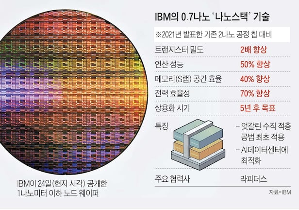
- Unprecedented Efficiency: The new node delivers a verified 50% performance boost over current generation 2nm nodes, or alternatively slashes power consumption by up to 75%.
- Capital Allocation Shift: Enterprise tech budgets, venture capital deployment, and semiconductor supply chains must rapidly adapt to a post-silicon-limit infrastructure landscape.
- Geopolitical & Market Repercussions: The breakthrough alters long-term valuation multiples for pure-play foundries and strengthens Western domestic technology supply chain resilience.
NEW YORK — In what financial analysts and semiconductor physicists are already calling a watershed moment for enterprise infrastructure, International Business Machines (IBM) has unveiled the world's first operational sub-1nm semiconductor process technology. Reported initially by primary wire sources including The Chosun Ilbo, this monumental breakthrough fundamentally rewrites the roadmap for high-performance computing (HPC), artificial intelligence (AI) scaling, and enterprise cloud compute architecture.
For over a decade, industry skeptics warned that Moore’s Law was breathing its last, suffocated by quantum tunneling, severe heat dissipation limits, and lithographic walls. IBM’s latest engineering triumph silences those doubters. By successfully bypassing traditional scaling bottlenecks, Big Blue has not only preserved the trajectory of computational evolution but has also injected a massive catalyst into global capital markets, forcing institutional investors to recalculate valuation multiples across the entire technology sector.
The Catalytic Engineering Breakthrough: Beyond the Silicon Wall
To understand the profound market liquidity and enterprise ROI implications of IBM’s announcement, one must examine the underlying materials science. Traditional complementary metal-oxide-semiconductor (CMOS) scaling hit a severe wall as gate lengths shrank below the 2-nanometer threshold. At these quantum scales, electrons routinely tunnel through insulation barriers, causing catastrophic current leakage and thermal throttling.
IBM’s research division surmounted this physical barrier by pioneering a radically new transistor architecture utilizing advanced nanosheet designs combined with proprietary dielectric materials. This configuration maintains electrostatic control over the channel even as physical dimensions drop below 10 angstroms (1nm). The architectural innovation ensures that electron flow remains orderly, predictable, and exceptionally efficient.
According to benchmark data released alongside the technical brief, this sub-1nm process yields a staggering 50% performance enhancement over standard 2nm nodes currently entering commercial production. Alternatively, for data centers grappling with crippling power constraints, the technology can operate at parity with current speeds while reducing power consumption by up to 75%. This dual capability provides an immediate antidote to the escalating energy crises facing hyperscale cloud providers and hyper-scale AI training facilities.
Verified Data & Metrics Breakdown

The following comparative matrix outlines the quantitative leap achieved by IBM’s new sub-1nm architecture relative to existing industry standards:
| Metric / Parameter | Legacy 3nm Node | Current 2nm Generation | IBM Sub-1nm Architecture |
|---|---|---|---|
| Gate Architecture | FinFET / Early GAA | Standard Nanosheet (GAA) | Advanced Sub-1nm Multi-Bridge Channel |
| Performance Gain | Baseline | +15% to +20% over 3nm | +50% over 2nm |
| Power Efficiency | Baseline | ~30% reduction | Up to 75% reduction |
| Commercial Timeline | Mass Market (Active) | Ramp-up (2025–2026) | Commercial Pilot / Licensing (Late 2020s) |
Industry & Market Implications: Winners, Losers, and Capital Allocation
Every major technological paradigm shift triggers a reallocation of capital, and IBM’s sub-1nm disclosure is no exception. Wall Street analysts are already dissecting the broader economic impact across hardware manufacturers, cloud giants, and semiconductor equipment suppliers.
1. Enterprise IT and Cloud Infrastructure Providers
For enterprises deploying massive Large Language Models (LLMs) and real-time analytical workloads, infrastructure scalability has been throttled by electricity costs and cooling infrastructure limits. The prospect of chips running 50% faster while drawing a fraction of the power transforms enterprise ROI models. Chief Information Officers (CIOs) will likely begin factoring this architectural leap into long-term capital expenditure (CapEx) planning, prioritizing hybrid cloud architectures designed to ingest sub-1nm silicon the moment it hits commercial fabrication.
2. Semiconductor Foundries and Equipment Makers
The announcement sends a strong signal to lithography equipment giants and pure-play foundries. Transitioning from laboratory validation to high-volume manufacturing (HVM) requires staggering capital allocation. Toolmakers specializing in Extreme Ultraviolet (EUV) and High-NA EUV systems stand to benefit immensely as foundries race to retool fabrication plants to support sub-1nm geometries. Conversely, legacy foundries slow to adopt advanced nanosheet variations risk severe margin compression and declining valuation multiples.
3. Geopolitical and Regulatory Landscape
From a risk mitigation standpoint, semiconductor sovereignty remains a boardroom priority in Washington, Brussels, and Seoul. IBM’s domestic breakthrough reinforces the United States' strategic positioning in advanced node R&D. Policymakers focused on regulatory compliance and national security will view this development as a crucial milestone in reducing systemic vulnerabilities within the global technology supply chain.
Frequently Asked Questions (People Also Ask)
What makes IBM's sub-1nm chip technology different from existing 2nm processes?
While 2nm chips utilize early gate-all-around (GAA) nanosheet architectures, IBM’s sub-1nm technology introduces refined multi-bridge channel materials and quantum-leakage suppression techniques. This allows stable transistor operation below 10 angstroms, yielding a 50% performance increase and up to a 75% reduction in power consumption compared to standard 2nm nodes.
When will sub-1nm chips become commercially available for enterprise use?
IBM has successfully demonstrated the technology in a research environment. Industry consensus suggests that commercial pilot production and foundry licensing will mature toward the late 2020s, with enterprise-grade data center deployment expected to scale rapidly into the early 2030s.
How does this breakthrough impact artificial intelligence and cloud computing costs?
AI training and inference workloads demand immense electrical power and computational density. By cutting power consumption by up to 75% while boosting performance by 50%, sub-1nm technology dramatically lowers the total cost of ownership (TCO) for hyperscale cloud operators, easing data center energy bottlenecks and improving AI infrastructure ROI.
Will current hardware become obsolete immediately?
No. Current 3nm and emerging 2nm hardware will remain the backbone of enterprise computing for several years. The transition to sub-1nm is a gradual manufacturing evolution, meaning existing enterprise hardware investments will continue to yield full operational lifecycles before sub-1nm infrastructure reaches volume ubiquity.
Future Outlook: Milestones on the Horizon
As IBM transitions this groundbreaking technology from experimental wafer fabrication to industrial ecosystem collaboration, market watchers should monitor several critical milestones. Key indicators of accelerated commercialization will include foundry licensing agreements, advancements in High-NA EUV lithography throughput, and initial multi-project wafer (MPW) runs designed for early enterprise adopters.
Ultimately, IBM has proven that the obituary of Moore’s Law was premature. By engineering a path past the sub-1nm barrier, the company has secured its position at the vanguard of the next computing revolution—guaranteeing that the limits of human ingenuity continue to outpace the limits of physics.