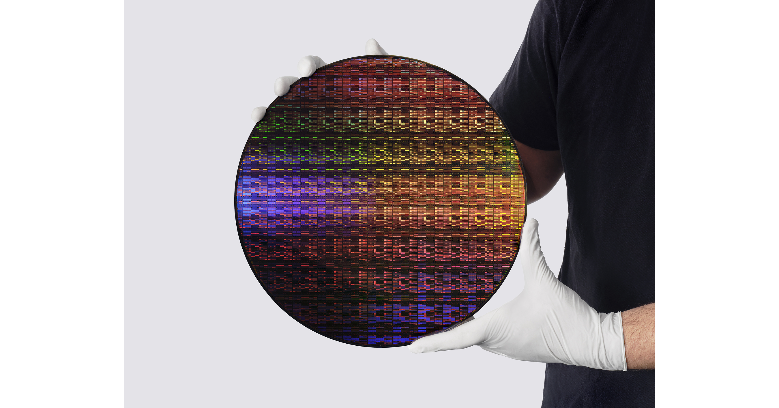
ARMONK, N.Y. — In what industry veterans are calling a watershed moment for modern computing, IBM has officially unveiled the world’s first sub-1 nanometer semiconductor technology. Announced on June 25, 2026, according to official dispatches from the IBM Newsroom, this monumental hardware leap breaks through physical scaling barriers that have challenged semiconductor physicists for over a decade. By defying traditional manufacturing limits, IBM’s latest engineering triumph promises to redefine the boundaries of artificial intelligence, mobile computing, and planetary-scale data infrastructure.
The newly unveiled architecture moves humanity past the fading era of conventional silicon scaling. Driven by soaring global demand for dense, high-performance compute engines—particularly for power-hungry generative AI models—this breakthrough introduces a radical paradigm shift in how microprocessors are built, powered, and cooled.
The Engineering Marvel: Inside the 'Nanostack' 3D Architecture
At the heart of IBM’s sub-1 nanometer breakthrough is a revolutionary architecture known as "nanostack" 3D chip design. Traditional planar and even early gate-all-around (GAA) architectures have faced severe quantum tunneling and leakage issues as transistors approached the single-nanometer threshold. IBM’s multidisciplinary research teams bypassed these roadblocks by engineering a vertically integrated, multi-layered stack that maximizes transistor density without sacrificing electron mobility.
According to specifications released by IBM hardware engineers, the new sub-1 nm chip packs nearly 100 billion transistors onto a single piece of silicon no larger than a human fingernail. This staggering density enables unprecedented computational parallelism, allowing processors to execute complex algorithmic calculations locally and instantaneously.
- Unprecedented Density: Nearly 100 billion functional transistors on a fingernail-sized die.
- Vertical Integration: Advanced "nanostack" 3D architecture overcomes traditional lateral scaling limits.
- Quantum Mitigation: Proprietary material science innovations successfully suppress electron leakage at sub-1 nm dimensions.
Unlocking Massive Power Savings for Generative AI

Beyond raw performance gains, the most disruptive implication of IBM’s new chip architecture centers on energy efficiency. The explosive growth of large-scale artificial intelligence models has placed an unsustainable burden on global electrical grids, with data centers consuming record amounts of power for cooling and inference processing.
IBM’s newest architecture could unlock massive, game-changing power savings for enterprise AI applications. By operating at drastically lower voltages while maintaining superior throughput, the sub-1 nm processors dramatically slash thermal dissipation. Industry analysts note that this thermal efficiency could soon eliminate the need for complex, power-hungry liquid cooling systems in next-generation enterprise server racks.
Key Metrics: How the Sub-1nm Architecture Compares
| Feature / Specification | Previous Generation (2nm Class) | IBM Sub-1 Nanometer Technology |
|---|---|---|
| Feature Node | ~2.0 Nanometers | Sub-1 Nanometer (<1nm) |
| Transistor Density | ~50 Billion per die | Nearly 100 Billion per die |
| Primary Architecture | Gate-All-Around (GAA) Nanosheet | "Nanostack" 3D Architecture |
| Target Workloads | General Compute & Early AI | High-Density Generative AI & Hyperscale Cloud |
Industry Reaction and Future Commercial Outlook
The announcement has sent ripples across Wall Street and global technology markets, where supply chain resiliency and semiconductor dominance dictate geopolitical and economic power. Major cloud providers and hardware manufacturers are already assessing licensing and foundry partnerships to integrate IBM’s breakthrough into upcoming enterprise product roadmaps.
"IBM's latest chip breakthrough marks a landmark moment not just for our company, but for the entire global technology ecosystem," senior engineering leadership stated in the primary wire release. "We are proving that Moore's Law is not dead—it has simply evolved into a third-dimensional reality."
While commercial mass production timelines will depend on foundry adoption and tool readiness over the next 24 to 36 months, the fundamental proof-of-concept is now a verified reality. As enterprises race to deploy autonomous agents and real-time generative models, IBM’s sub-1 nanometer architecture provides the vital hardware foundation required for the next decade of digital transformation.
Frequently Asked Questions
What makes IBM's sub-1 nanometer chip technology different from previous generations?
Unlike traditional 2nm or 3nm chips that rely primarily on lateral scaling and GAA nanosheets, IBM's technology utilizes a proprietary "nanostack" 3D architecture. This allows roughly 100 billion transistors to be packed onto a fingernail-sized die while successfully mitigating quantum leakage issues.
When will these sub-1 nanometer chips be available commercially?
While IBM has successfully debuted and verified the technology as of June 2026, commercial integration into enterprise data centers and consumer hardware is anticipated to ramp up over the next few years as foundry ecosystems adapt to the new 3D manufacturing standards.