Executive Takeaways
- Manufacturing Convergence: Interuniversity Microelectronics Centre (Imec) has successfully fabricated the world's first quantum dot qubit device utilizing High-Numerical Aperture Extreme Ultraviolet (High-NA EUV) lithography.
- Timeline Compression: By adapting 300mm silicon fabrication lines built for next-generation AI accelerators, quantum computing bypasses decades of custom, low-yield manual assembly.
- Capital Allocation Shift: Enterprise ROI models for quantum infrastructure are radically accelerated, prompting institutional investors to re-evaluate valuation multiples across both pure-play quantum startups and legacy semiconductor foundries.
- Ecosystem Disruption: Standardized CMOS compatibility allows quantum processors to leverage existing EDA (Electronic Design Automation) software, cloud compute architectures, and lithography supply chains dominated by ASML.
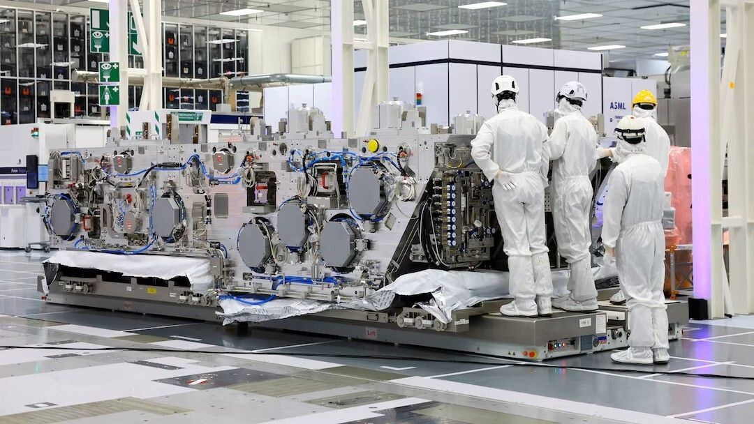
LEUVEN, BELGIUM — In a development quietly circulating through elite engineering corridors and now confirmed by primary technical wire sources, the Interuniversity Microelectronics Centre (Imec) has crossed a Rubicon that semiconductor and quantum physicists have debated for over twenty years. By successfully manufacturing a quantum dot qubit device using ASML’s bleeding-edge High-Numerical Aperture Extreme Ultraviolet (High-NA EUV) lithography toolset, Imec has effectively welded the notoriously idiosyncratic roadmap of quantum computing to the hyper-efficient, high-yield assembly lines of mainstream artificial intelligence processors.
For institutional investors, enterprise tech strategists, and sovereign risk analysts, the implications cannot be overstated. For decades, the Achilles' heel of quantum computing has not been theoretical physics, but industrial scalability. While brilliant academic labs could fabricate isolated, high-coherence qubits using custom electron-beam lithography, scaling those architectures to the millions required for fault-tolerant error correction felt akin to hand-crafting cathedral stained glass in the era of automated commercial printing. Imec’s breakthrough shatters that bottleneck. By proving that spin qubits can be patterned with the sub-nanometer precision of sub-3nm gate-all-around (GAA) logic transistors on standard 300mm silicon wafers, the industry has compressed its commercialization timeline by an estimated five to seven years.
The Catalytic Convergence: Why High-NA EUV Changes Everything
To understand the magnitude of Imec’s announcement, one must examine the economic and physical realities of modern semiconductor manufacturing. Traditional Extreme Ultraviolet (EUV) lithography—operating at a 13.5-nanometer wavelength with a 0.33 numerical aperture—has been the workhorse of advanced nodes, powering everything from Apple’s M-series silicon to NVIDIA’s Hopper and Blackwell AI architectures. However, as transistor geometries shrink below the 2nm threshold, and as quantum engineers attempt to pack dense arrays of quantum dots onto silicon substrates, 0.33 NA EUV hits severe diffraction and overlay limits.
Enter High-NA EUV (0.55 NA systems, priced upwards of $350 million per unit). By increasing the numerical aperture, ASML’s new optical system projects light with sharper fidelity, enabling single-exposure feature patterning that previously required complex, yield-killing multi-patterning techniques. Imec leveraged this optical leap to define nanoscale gate electrodes and confinement structures for silicon spin qubits with unprecedented dimensional control.
Silicon spin qubits—trapped electrons or holes in quantum dots defined by metal gates on silicon—have long been prized for their potential compatibility with traditional complementary metal-oxide-semiconductor (CMOS) manufacturing. Unlike superconducting circuits that require sprawling dilution refrigerators and macro-scale coaxial wiring, silicon spin qubits operate at slightly higher temperatures (around 1 Kelvin) and share a structural lineage with modern microprocessors. However, translating theoretical CMOS-compatibility into a functional 300mm fab run has been plagued by atomic-scale defects, charge noise, and gate-pitch limitations.
By applying High-NA EUV, Imec engineers achieved sub-nanometer critical dimension (CD) uniformity across a full 300mm wafer. This precision eliminates the statistical variations in quantum dot confinement potentials that previously caused qubit frequency drift and decoherence. In simple terms: Imec has made quantum dots behave with the relentless, predictable consistency of standard logic gates.
Comparative Analysis: Legacy Quantum Fabrication vs. Imec High-NA EUV Paradigm
| Metric / Parameter | Legacy / Custom Fabrication | Imec High-NA EUV Silicon Spin Qubit Approach |
|---|---|---|
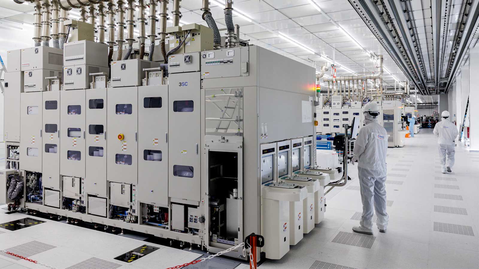
| Wafer Substrate Size | Small pieces / R&D substrates (often < 100mm) | Standard industrial 300mm semiconductor wafers |
| Lithography Toolset | E-beam lithography / Low-NA EUV (0.33 NA) | Next-Gen High-NA EUV (0.55 NA) |
| Integration with AI Logic | Zero; completely isolated manufacturing stack | Native co-integration on shared 300mm CMOS lines |
| Yield & Repeatability | Low yield, high variance, manual tuning required | High-volume manufacturing (HVM) foundry standards |
| Capital Intensity & ROI Model | Venture-funded boutique cleanrooms, high capex per unit | Leverages existing multi-billion-dollar fab depreciation schedules |
Macroeconomic & Market Implications: Winners, Losers, and Capital Allocation
The convergence of quantum device fabrication with mainstream semiconductor infrastructure triggers profound structural shifts across the enterprise technology landscape. Venture capital allocation, corporate treasury strategies, and sovereign technology funds must immediately recalibrate their risk mitigation models.
1. The Foundry Hegemony Wins Again
Pure-play quantum computing startups that relied on proprietary, non-standard manufacturing techniques now face an existential choice: pivot to CMOS-compatible silicon spin architectures or risk obsolescence. Foundries with advanced lithography access—specifically Taiwan Semiconductor Manufacturing Company (TSMC), Intel Foundry, and Samsung—along with equipment titans like ASML, find their economic moats infinitely deepened. Because Imec’s process runs on standard equipment sets, foundries can theoretically allocate a sliver of their existing 300mm fab capacity to trial quantum chip production without spinning up entirely greenfield cleanrooms.
2. Cloud Compute Architecture and Hybrid AI-Quantum Systems
The enterprise ROI for quantum computing has historically been clouded by questions of data integration. How does a quantum processor interface with the classical GPU clusters handling massive LLM workloads? By embedding quantum dots directly onto silicon architectures that mirror advanced logic layout rules, the physical barriers to heterogeneous integration vanish. We are moving rapidly toward a future where enterprise cloud providers (AWS, Microsoft Azure, Google Cloud) will offer hybrid server racks containing traditional AI accelerators tightly coupled with silicon spin-qubit co-processors via high-bandwidth optical interconnects.
3. Regulatory Compliance, Export Controls, and Geopolitics
Because High-NA EUV technology is already subject to stringent geopolitical export controls and multilateral trade restrictions, tying the future of quantum computing directly to this machinery places quantum hardware squarely inside the inner sanctum of national security technology. Sovereign states lacking access to ASML’s 0.55 NA systems will face an insurmountable barrier in scaling fault-tolerant quantum processors, altering global valuation multiples and defense readiness indexes.
Frequently Asked Questions (People Also Ask)
What makes Imec’s use of High-NA EUV for quantum dots different from previous methods?
Previous quantum dot devices were primarily patterned using electron-beam (e-beam) lithography or older 0.33 NA EUV systems. E-beam is serial, slow, and incapable of high-volume manufacturing. High-NA EUV (0.55 NA) allows parallel, single-exposure patterning with sub-nanometer precision across entire 300mm wafers, matching the exact dimensional tolerances used to manufacture advanced AI logic processors.
Why are silicon spin qubits considered superior for industrial scaling compared to other modalities?
Silicon spin qubits utilize the existing infrastructure, materials science, and cleanroom protocols of the trillion-dollar semiconductor industry. Unlike superconducting qubits or trapped ions that require bespoke, exotic manufacturing environments and manual packaging, silicon spin qubits can theoretically be mass-produced in standard commercial silicon foundries.
How does this breakthrough impact enterprise timelines for commercial quantum computing?
By bridging the gap between laboratory physics and high-volume semiconductor manufacturing (HVM), Imec’s breakthrough removes the primary bottleneck to scaling qubit counts. Industry analysts estimate this collapses the timeline for commercially viable, fault-tolerant quantum systems by five to seven years, shifting enterprise risk strategies from long-term basic research to immediate infrastructure planning.
Will this make existing quantum startups obsolete?
Not necessarily obsolete, but it forces a strategic realignment. Startups focusing purely on software, algorithms, or unique error-correction protocols will benefit immensely. However, hardware startups relying on custom, non-CMOS manufacturing processes will face immense capital pressure as foundry-backed silicon spin architectures achieve superior manufacturing yields and economies of scale.
Future Outlook: Milestones on the Road to 2030
As the dust settles on Imec’s announcement, the executive focus shifts from proof-of-concept to execution velocity. Over the next 24 to 36 months, industry watchers must track three critical operational milestones:
- Yield Stability at Scale: Demonstration of multi-qubit entanglement uniformity across entire 300mm wafers with error rates low enough to initiate surface-code error correction.
- Heterogeneous Packaging Integration: Successful wire-bonding or monolithic 3D stacking of high-density silicon spin processors alongside classical cryogenic control chips (CMOS cryogenic controllers).
- <Foundry Commercialization Announcements: Formal technology transfer agreements between Imec, research consortia, and tier-1 commercial foundries to pilot multi-project wafer (MPW) runs for enterprise clients.
Imec has effectively closed the chapter on quantum computing as an isolated scientific curiosity. By plugging quantum hardware into the relentless machinery of modern semiconductor manufacturing, the countdown to enterprise-scale quantum supremacy has officially accelerated.