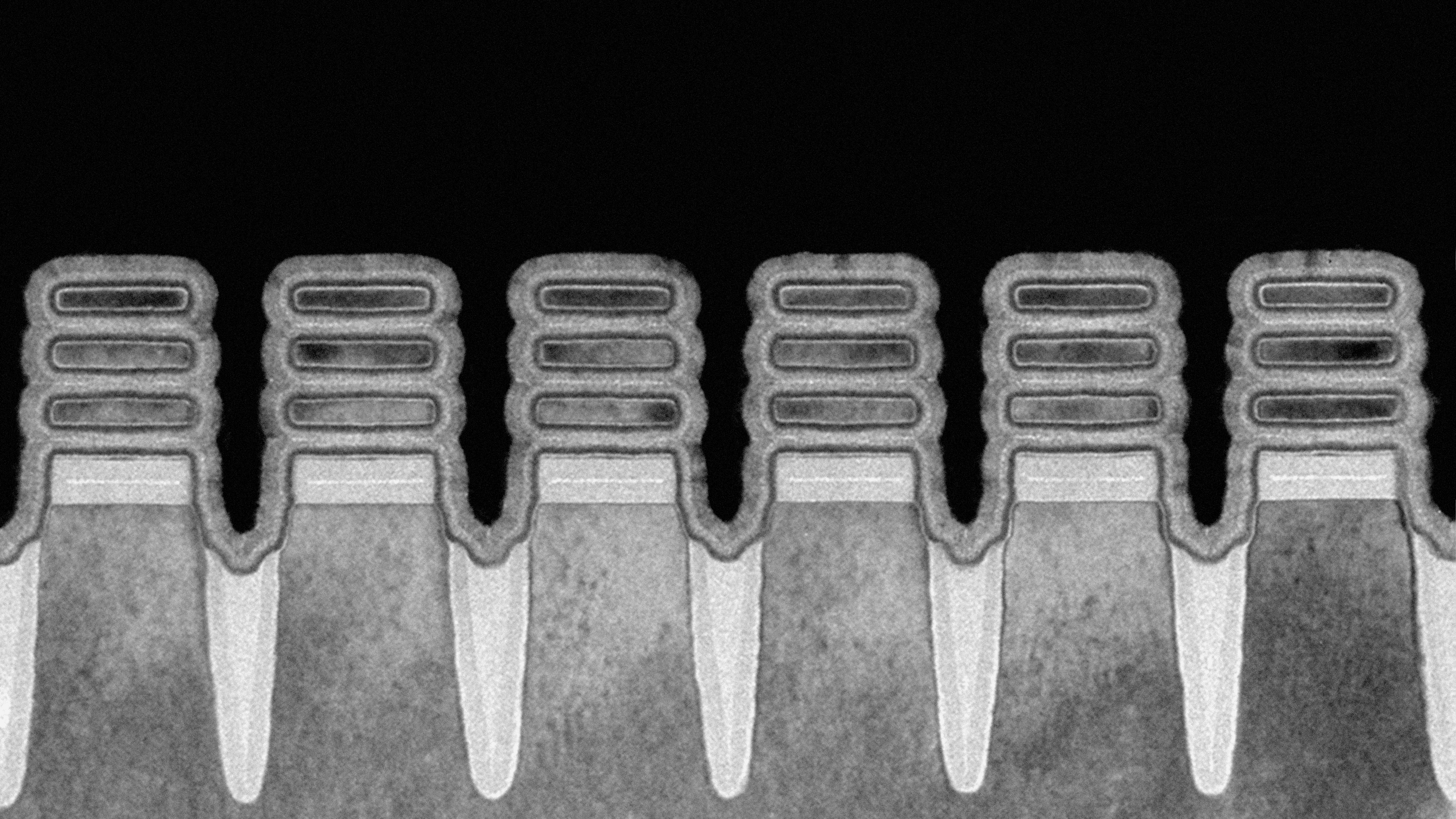
ALBANY, N.Y. — In the high-stakes theater of global semiconductor manufacturing, where nanometers represent billions of dollars in market valuation multiples and geopolitical leverage, Big Blue has just detonated a seismic technological charge. IBM Research has officially pulled back the curtain on the world’s first functional 2-nanometer (nm) node test chip, packing an astonishing 50 billion transistors onto a piece of silicon no larger than a fingernail.
Unveiled at the Global Research Center in Albany, New York, this milestone marks a monumental pivot point in enterprise computing infrastructure, cloud compute architecture, and capital allocation strategies worldwide. As global supply chains grapple with structural fragilities and skyrocketing energy demands from generative artificial intelligence and hyperscale data centers, IBM’s breakthrough promises a radical leap in power efficiency and performance density. For enterprise decision-makers, private equity investors, and risk mitigation strategists, understanding the anatomy of this 2nm architecture is no longer optional—it is a core prerequisite for forecasting the next decade of digital transformation and enterprise ROI.
Executive Takeaways
Test Our Free AI & Tech Utilities Suite
Calculate LLM API token costs, analyze article dwell-time, or simulate tech DCA returns.
- Unprecedented Density: IBM’s new 2nm test chip successfully integrates 50 billion microscopic switches onto a footprint roughly the size of a fingernail, achieving a transistor density of 333 million transistors per square millimeter.
- Revolutionary Architecture: The breakthrough relies on nanosheet (gate-all-around or GAA) architecture rather than traditional FinFET designs, overcoming severe quantum mechanical leakage barriers at sub-3nm scales.
- Massive Efficiency Gains: The 2nm node delivers up to 45 percent higher performance or 75 percent lower power consumption compared to prevailing commercial 7nm node chips deployed across enterprise data centers today.
- Strategic Geopolitical & Supply Chain Ripple Effects: While manufacturing commercialization remains on the horizon for mid-decade deployment, the breakthrough underscores the critical role of domestic R&D consortiums in securing long-term technology infrastructure scalability and national tech sovereignty.
The Anatomy of a Quantum-Era Leap: Breaking the 2nm Barrier

For decades, Moore’s Law—the empirical observation that the number of transistors on a microchip doubles roughly every two years—has faced mounting thermodynamic and quantum mechanical walls. As semiconductor geometries shrink below the 5nm and 3nm thresholds, traditional planar and FinFET transistor architectures suffer from severe current leakage, thermal throttling, and unpredictable electron tunneling. At these atomic scales, controlling the flow of electricity becomes akin to stopping water with a picket fence.
IBM’s research team, operating out of the Albany NanoTech Complex in New York, bypassed these fundamental physical roadblocks by pioneering a bottom-up redesign of the transistor itself. Rather than relying on standard FinFET structures, IBM implemented a vertical nanosheet architecture. In this configuration, the gate material completely surrounds the channel on all four sides—commonly referred to as Gate-All-Around (GAA)—maximizing electrostatic control over the channel and effectively sealing off current leakage.
"The IBM chip announced today reflects the ingenuity of IBM and its unwavering commitment to hard tech innovation," said Darío Gil, Senior Vice President and Director of IBM Research. "It is emblematic of our ability to collaborate across the ecosystem and drive breakthroughs that translate into tangible economic value and infrastructure scalability for our clients."
To achieve the staggering density of 50 billion transistors, IBM engineers integrated a proprietary bottom-up dielectric gate-all-around (DB-GAA) nanosheet structure. This manufacturing feat allows gate lengths to shrink down to a staggering 12 nanometers while maintaining pristine channel integrity. For enterprise technology buyers, this engineering triumph translates directly into tangible operational metrics: servers built on this architecture can potentially run workloads at a fraction of the electricity currently consumed by hyperscale data centers, slashing operational expenditure (OpEx) and mitigating carbon compliance risks.
Verified Data & Metrics Breakdown Table
| Metric / Specification | Conventional Commercial 7nm Node | IBM Research 2nm Test Chip | Performance Delta / Strategic Advantage |
|---|---|---|---|
| Transistor Density | ~90 to 100 million transistors / mm² | ~333 million transistors / mm² | Over 3x increase in computational density per square millimeter. |
| Total Transistor Count (Test Die) | Varies (typically < 20B on consumer dies) | 50 Billion transistors on a fingernail-sized die | Unprecedented parallel processing capabilities for heavy AI/ML workloads. |
| Power Efficiency | Baseline reference | 75% lower power consumption at matching performance | Massive reduction in data center cooling costs and enterprise carbon footprint. |
| Raw Performance Gain | Baseline reference | Up to 45% higher performance at matching power | Accelerated transaction processing and complex financial modeling capabilities. |
| Architectural Foundation | FinFET (Fin Field-Effect Transistor) | Nanosheet Gate-All-Around (GAA) | Superior electrostatic control, eliminating sub-3nm quantum leakage. |
Industry & Market Implications: Re-Engineering the Global Tech Stack
The unveiling of IBM’s 2nm test chip sends powerful shockwaves through the global semiconductor ecosystem, altering valuation multiples, capital expenditure forecasts, and competitive positioning across the enterprise hardware landscape.
Enterprise ROI and Cloud Compute Architecture
For Chief Information Officers and enterprise cloud architects, the primary bottleneck in scaling artificial intelligence, large language models (LLMs), and high-frequency algorithmic trading infrastructure has shifted from compute capacity to thermal dissipation and power availability. Data centers are rapidly approaching local grid capacity limits. By delivering a 75% reduction in power consumption, 2nm-based server processors will fundamentally alter enterprise Total Cost of Ownership (TCO). Cloud service providers adopting these nodes will enjoy superior margin expansion, lower infrastructure maintenance outlays, and enhanced capability to host dense, power-hungry neural network training clusters.
Competitive Dynamics and Capital Allocation
While industry giants like TSMC, Samsung, and Intel are locked in a fierce, multi-billion-dollar race toward commercial sub-3nm and 2nm mass production, IBM’s business model relies heavily on joint development alliances and intellectual property licensing. By proving out the viability of nanosheet GAA architecture in a laboratory setting, IBM validates the roadmap for its foundry partners—including Samsung and Intel, both of which have licensed IBM research breakthroughs in the past. This collaborative R&D ecosystem model acts as a powerful risk-mitigation strategy, pooling capital expenditure across multiple industrial players.
Geopolitical Resilience and Supply Chain Security
In an era defined by geopolitical friction over semiconductor fabrication choke points in East Asia, domestic R&D breakthroughs anchored in New York state carry profound national security and economic liquidity implications. Governments are actively deploying sovereign capital subsidies—such as the U.S. CHIPS and Science Act—to ensure that next-generation manufacturing technology remains rooted in allied jurisdictions. IBM’s Albany facility continues to serve as the crown jewel of American semiconductor R&D, bridging the gap between academic theory and industrial fabrication reality.
Frequently Asked Questions (People Also Ask)
What is a 2nm chip, and why is it important?
A 2nm chip refers to a semiconductor manufacturing node where key features of the transistors measure approximately 2 nanometers in width—roughly the size of a strand of DNA. It is critically important because shrinking transistors allows manufacturers to cram tens of billions more switches onto a single piece of silicon, resulting in massive leaps in processing speed, energy efficiency, and data center sustainability.
How does IBM’s 2nm chip differ from current 7nm or 5nm chips?
Unlike current 7nm and 5nm chips that predominantly use FinFET (Fin Field-Effect Transistor) architecture, IBM’s 2nm chip utilizes a Gate-All-Around (GAA) nanosheet design. This architectural shift wraps the electrical gate on all four sides of the channel, preventing current leakage and quantum mechanical interference that plagues smaller nodes, enabling a staggering density of 333 million transistors per square millimeter.
When will 2nm chips be commercially available in enterprise servers and devices?
While IBM successfully demonstrated a working prototype in May 2021, transitioning a laboratory test chip into high-volume commercial manufacturing typically requires a multi-year maturation cycle. Major foundries and enterprise hardware vendors are targeting commercial deployment in the mid-to-late 2020s, as extreme ultraviolet (EUV) lithography tools and fab cleanrooms are upgraded to handle sub-3nm production yields.
Will 2nm technology reduce carbon emissions in cloud data centers?
Yes. Because IBM’s 2nm architecture delivers up to 75% lower power consumption at equivalent performance levels compared to standard 7nm chips, hyperscale data centers transitioning to these processors will experience a dramatic reduction in electricity demand and cooling requirements, directly advancing corporate sustainability goals and regulatory compliance mandates.
Future Outlook: Navigating the Road to Commercialization
The journey from a successful laboratory prototype in Albany to mass-market commercialization is fraught with formidable engineering hurdles. The primary challenge moving forward lies in manufacturing yield optimization—ensuring that wafer defect rates are low enough to make mass production economically viable. This requires perfecting High-Numerical Aperture Extreme Ultraviolet (High-NA EUV) lithography tools, which cost upwards of $350 million per unit.
As enterprise clients demand ever-greater computing power to fuel autonomous systems, real-time quantum-safe cryptography, and enterprise-grade generative AI, the imperative for sub-3nm silicon will only accelerate. IBM’s 2nm breakthrough has established a definitive technological ceiling—and a roadmap—for the global semiconductor industry. For market participants, investors, and enterprise tech leaders, the message is unambiguous: the nanoscale revolution is no longer a theoretical horizon; it is the foundational architecture upon which the next century of enterprise infrastructure will be built.