Executive Takeaways
- Unprecedented Density: IBM Research successfully prototyped the world’s first 2-nanometer (nm) nanosheet semiconductor test chip, packing an astonishing 50 billion transistors onto a die roughly the size of a fingernail (150 square millimeters).
- Paradigm-Shifting Efficiency: The architecture delivers up to 45% higher performance or 75% lower energy consumption compared to mainstream 7nm node technology, directly altering enterprise infrastructure scalability and cloud compute architecture economics.
- Capital Allocation and Supply Chain Impact: Coming out of the Albany Nanotech Complex, this breakthrough positions IBM to alter global foundry dynamics, pressuring competitors while redefining risk mitigation and valuation multiples across the semiconductor value chain.
- Next-Gen Enterprise ROI: The technology promises transformative efficiency gains for power-hungry workloads including artificial intelligence, 5G/6G cellular infrastructure, autonomous systems, and data center operations.
NEW YORK — In an era defined by relentless demands for computing power and the looming physical boundaries of silicon scaling, IBM Research delivered a watershed moment for the global technology landscape. Announced from the Albany Nanotech Complex, IBM unveiled the world’s first functioning 2-nanometer (nm) semiconductor test chip. By successfully engineering a device that crams 50 billion microscopic switches onto a footprint no larger than a fingernail, Big Blue demonstrated that Moore’s Law is not dead—it is merely evolving through radical architectural engineering.
For enterprise technology leaders, chief financial officers, and semiconductor strategists, this announcement is far more than a laboratory curiosity. It represents a fundamental recalibration of capital expenditure, energy efficiency, and infrastructure scalability. As global data centers consume an escalating percentage of the world’s power grid, the arrival of a chip promising a 75% reduction in energy consumption over current 7nm commercial nodes offers a vital blueprint for sustainable, high-performance computing.
The Anatomy of a Breakthrough: Scaling Beyond 7nm and 5nm
Test Our Free AI & Tech Utilities Suite
Calculate LLM API token costs, analyze article dwell-time, or simulate tech DCA returns.
To understand the magnitude of IBM’s achievement, one must examine the physics of modern semiconductor manufacturing. For decades, the industry relied on FinFET (Fin Field-Effect Transistor) architecture, a design that allowed chips to scale downward from the 22nm era through 14nm, 10nm, and 7nm. However, as gate lengths shrink below the 5nm threshold, traditional FinFET structures encounter severe quantum mechanical leakage issues, where electrons tunnel through barriers they are supposed to block, causing massive power waste and thermal dissipation failures.
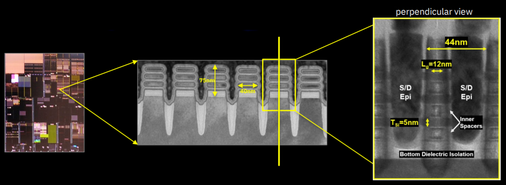
IBM circumvented this physical wall by pioneering a gate-all-around (GAA) nanosheet architecture. Instead of vertical fins, IBM’s 2nm design utilizes horizontal silicon nanosheets stacked vertically. By wrapping the gate material entirely around these sheets, engineers achieved complete electrostatic control over the channel. This innovation allowed IBM to reduce the nanosheet width down to 15nm while packing 50 billion transistors into a 150-square-millimeter die.
The manufacturing process required unprecedented precision, utilizing extreme ultraviolet (EUV) lithography layers combined with proprietary bottom-up dielectric isolation gate-all-around processing. The resulting test chip proves that scaling down to the 2nm threshold is industrially viable, paving the way for commercial foundry production that can sustain exponential compute growth without incurring unsustainable energy penalties.
Verified Data & Metrics Breakdown
| Metric / Specification | IBM 2nm Test Chip | Mainstream 7nm Nodes | Comparative Gain / Impact |
|---|---|---|---|
| Transistor Count | 50 Billion | ~10 to 30 Billion (Typical) | Significantly higher compute density |
| Die Size | ~150 mm² (Fingernail size) | Variable (100–300 mm²) | Optimized wafer yield efficiency |
| Performance Gain | Up to 45% higher at same power | Baseline | Substantial processing throughput boost |
| Energy Efficiency | 75% lower power consumption | Baseline | Massive reduction in data center cooling overhead |
| Architecture Type | Gate-All-Around (GAA) Nanosheet | FinFET | Superior electrostatic channel control |
Industry & Market Implications: Winners, Losers, and Economic Realities
In the high-stakes arena of global semiconductor manufacturing, technological breakthroughs directly translate into market liquidity, valuation multiples, and geopolitical leverage. IBM’s announcement reverberates across multiple financial and industrial sectors:
- Enterprise Data Centers and Hyperscalers: Cloud providers—including Amazon Web Services, Microsoft Azure, and Google Cloud—face soaring electricity bills and carbon emission caps. Transitioning server architectures to 2nm nodes can dramatically lower power usage effectiveness (PUE) metrics, yielding superior enterprise ROI on hardware refresh cycles.
- Mobile and Edge Computing: For smartphone manufacturers and edge AI developers, a 75% reduction in power consumption translates to battery life that could extend from hours to multiple days, even while running complex on-device machine learning models.
- Foundry Ecosystem and Supply Chain Risk Mitigation: While IBM operates on a joint-development model rather than mass-market high-volume foundry fabrication (partnering with ecosystem giants like Samsung and Intel), this breakthrough validates GAA technology as the definitive successor to FinFET. This influences capital allocation strategies across the globe as foundries race to retool multi-billion-dollar fabrication plants.
- Geopolitical and Regulatory Compliance: Advanced node research occurring within domestic U.S. research consortia reinforces national security objectives regarding semiconductor supply chain sovereignty, aligning with legislative frameworks aimed at reshoring critical electronics manufacturing.
Frequently Asked Questions (People Also Ask)
What is a 2nm semiconductor chip, and why is it important?
A 2nm chip refers to a semiconductor manufacturing node where features on the integrated circuit are approximately 2 nanometers in scale. It is important because shrinking transistors allows manufacturers to pack billions more switches onto a single piece of silicon, dramatically increasing processing speed while lowering electrical resistance and power consumption.
How does IBM’s 2nm design differ from current chips?
Most commercial chips today rely on FinFET architecture. IBM’s 2nm breakthrough utilizes a gate-all-around (GAA) nanosheet architecture. This design wraps the gate material on all four sides of the silicon channel, overcoming the severe electrical leakage issues that occur when traditional FinFET transistors are scaled below the 5nm threshold.
When will 2nm chips be available in commercial devices and servers?
While IBM successfully demonstrated a functioning test chip, commercial high-volume manufacturing (HVM) typically requires 2 to 4 years of refinement within semiconductor foundries. Industry roadmaps suggest commercial integration into high-performance enterprise servers, cloud infrastructure, and mobile devices will ramp up toward the middle of the decade.
What are the primary economic and environmental benefits of 2nm technology?
The primary benefits are a 45% increase in computational performance at the same power level, or a 75% reduction in energy consumption compared to 7nm chips. For enterprises, this lowers data center operational expenditures (OpEx), reduces cooling requirements, and helps corporations meet strict environmental sustainability and carbon-neutrality mandates.
Future Outlook: Milestones on the Road to Commercialization
As the semiconductor industry digests IBM’s achievement, the focus shifts immediately to execution and yield optimization. Transitioning a laboratory test chip into mass production at scale requires overcoming significant hurdles in EUV pellicle durability, defect reduction, and packaging innovations such as 3D chip stacking.
Key financial and technical milestones to watch over the next 24 to 36 months include:
- Foundry Integration Roadmaps: Monitoring capital expenditure announcements by major foundry operators (such as TSMC, Samsung, and Intel) regarding commercial GAA production schedules.
- EDA Tool Readiness: Electronic Design Automation (EDA) software vendors releasing verified toolsets that allow chip designers to simulate and layout circuits specifically optimized for nanosheet physics.
- Enterprise Pilot Deployments: Early adopter announcements from hyperscale cloud providers testing 2nm-derived ASICs for specialized artificial intelligence training and inference workloads.
Ultimately, IBM’s 2nm milestone reaffirms that the ingenuity of materials science and semiconductor engineering continues to outpace premature obituaries of Moore’s Law. For enterprise leaders navigating digital transformation, the message is unequivocal: the next generation of hyper-efficient, high-performance computing is rapidly approaching the horizon.