Executive Takeaways
- Capital Allocation & State Backing: India's semiconductor roadmap has transitioned from conceptual policy to aggressive capital deployment, anchored by multi-billion-dollar incentives under the modified Semicon India program.
- Enterprise Integration: Domestic heavyweights, including Tata Consultancy Services (TCS), are launching custom silicon design ecosystems specifically tailored for high-growth verticals like automotive and industrial IoT.
- Global Supply Chain Diversification: Multinational foundries and equipment manufacturers are aggressively hedging geographic risk, positioning the subcontinent as a viable alternative to traditional East Asian manufacturing hubs.
- Infrastructure & Talent Scalability: Despite unprecedented state support and foreign direct investment (FDI), long-term viability hinges on overcoming structural deficits in ultra-pure water access, uninterrupted power grids, and advanced packaging engineering talent.
NEW DELHI — When the doors opened at SEMICON India 2026, the subtext of the global technology summit was unmistakable: the geopolitical map of microelectronics is being aggressively redrawn. Coming against a backdrop of tightening supply chain vulnerabilities and surging enterprise demand for specialized silicon, this year’s conclave in the national capital served as both a progress report and a stress test for New Delhi’s ambitious industrial policy.
For decades, India played a vital yet subordinate role in the global semiconductor value chain—dominating software architecture, integrated circuit (IC) design, and verification, while importing nearly 100% of its physical hardware. Today, driven by sweeping regulatory compliance incentives, sovereign risk mitigation strategies, and aggressive capital allocation from both domestic conglomerates and global foundries, that paradigm is fracturing. As highlighted by dispatches from the ground on September 16, 2026, the discourse has shifted decisively from if India can build a domestic chip ecosystem to how fast it can scale infrastructure to meet surging valuation multiples and market liquidity demands.
The Catalytic Shift: From Blueprint to Foundry Floor
Test Our Free AI & Tech Utilities Suite
Calculate LLM API token costs, analyze article dwell-time, or simulate tech DCA returns.
The journey to SEMICON India 2026 was paved with severe macroeconomic and geopolitical lessons. The post-pandemic supply chain crunches exposed the fragility of hyper-concentrated manufacturing nodes in East Asia, prompting Western and Asian democracies alike to prioritize technological sovereignty. India’s response was the rollout of its comprehensive semiconductor incentive packages, designed to de-risk capital expenditures for Tier-1 equipment makers and OSAT (Outsourced Semiconductor Assembly and Test) providers.
However, policy ambition alone does not manufacture silicon. The true inflection point arrived when foundational capital commitments materialized on the ground. Joint ventures pairing domestic industrial titans with legacy international chipmakers began transitioning from memorandum-of-understanding (MoU) stage to physical groundbreakings in Gujarat, Karnataka, and Tamil Nadu.
A striking example of this indigenous momentum showcased at the 2026 summit was TCS launching custom chip design frameworks specifically optimized for the automotive and semiconductor sectors. By moving up the value chain from legacy IT services to proprietary silicon architecture, Indian enterprises are capturing higher enterprise ROI and securing sticky, long-term vendor relationships with global original equipment manufacturers (OEMs).
Ecosystem Dynamics: Analyzing the Stakeholders
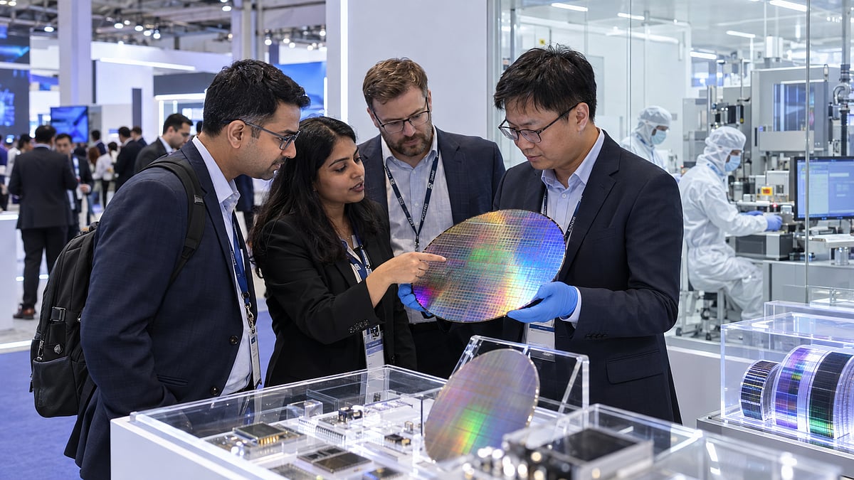
To understand the trajectory of India's semiconductor ambitions, one must examine the shifting dynamics across the tripartite pillars of the industry: government policy, enterprise execution, and global foundry integration.
1. Government Incentives and Fiscal Risk Mitigation
The Ministry of Electronics and Information Technology (MeitY) has refined its fiscal frameworks to offer up to 50% capital expenditure support for semiconductor fabrication units, display fabs, and compound semiconductor facilities. This aggressive subsidization is designed to offset the high initial capital expenditure (CapEx) and long payback periods inherent in semiconductor manufacturing. Regulatory compliance has been streamlined through single-window clearances, though bureaucratic friction remains a localized hurdle for foreign investors managing complex cross-border joint ventures.
2. Domestic Giants and Custom Silicon Innovation
While fabrication grabs the headlines, the real margin capture lies in specialized design and advanced packaging. Indian IT majors and agile fabless startups are leveraging their deep engineering pools to design application-specific integrated circuits (ASICs) for electric vehicles (EVs), telecommunications, and edge AI. The rollout of custom chip design platforms by firms like TCS signals a maturing market capable of supporting the entire lifecycle of a chip—from RTL (Register-Transfer Level) design to physical tape-out.
3. Global Partnerships and Geopolitical Hedging
Major international players view India not merely as a burgeoning consumer market, but as a critical node in their "China+1" risk mitigation strategies. Partnerships involving US, Japanese, and European semiconductor equipment manufacturers are transferring vital technological know-how, ensuring that India’s nascent fabs are integrated into established global supply chains rather than operating in isolation.
Verified Data & Metrics Breakdown
The following metrics outline the macroeconomic scale, targeted investments, and strategic milestones driving India's semiconductor push as evaluated at SEMICON India 2026:
| Metric / Parameter | Current Status (2026) | Strategic Implication / Target |
|---|---|---|
| Total Committed Outlay | ~$15 Billion + (Public-Private) | Covers initial fabs, OSAT facilities, and design-linked incentives (DLI). |
| Target Node Technology | 28nm to 65nm mature nodes (scaling to advanced nodes post-2028) | Meets high-volume demand for automotive, power electronics, and IoT. |
| Talent Pipeline | ~85,000 specialized engineers targeted by 2027 | Addresses global engineering deficits through specialized academic curricula. |
| Key Vertical Focus | Automotive, Industrial IoT, Telecommunications | Captures immediate domestic demand and high-margin industrial applications. |
Industry & Market Implications: Winners and Losers
The structural transformation catalyzed by SEMICON India 2026 carries profound market implications across asset classes and geographic regions:
- Winners — Specialized Fabless Startups and Design Houses: Companies possessing proprietary IP in analog, mixed-signal, and automotive semiconductors are seeing compressed funding cycles and surging valuation multiples as venture capital shifts toward hard-tech.
- Winners — Real Estate and Industrial Infrastructure Providers: Specialized industrial parks equipped with uninterrupted power supply (UPS), high-grade water treatment facilities, and secure logistics corridors in states like Gujarat and Tamil Nadu are capturing massive enterprise lease volumes.
- Losers — Purely Import-Dependent Trading Intermediaries: Traditional hardware importers who add minimal value between foreign foundries and domestic OEMs face margin compression as direct-to-enterprise manufacturing models take root.
- The Structural Risk Factor: While capital availability is robust, the ultimate bottleneck remains talent retention and resource sustainability. Semiconductor fabrication demands hyper-pure water and zero-tolerance power grids. Regional municipal bodies must scale infrastructure rapidly to prevent operational bottlenecks that could erode projected enterprise ROI.
Frequently Asked Questions (People Also Ask)
1. What are the core objectives of the SEMICON India 2026 initiative?
The primary objectives are establishing domestic semiconductor fabrication (fab) and OSAT facilities, reducing reliance on raw chip imports, fostering indigenous chip design capabilities for automotive and industrial sectors, and integrating India deeply into the trusted global semiconductor supply chain through lucrative state incentives.
2. Which nodes and manufacturing technologies are currently being prioritized in India?
India is initially prioritizing mature and legacy nodes ranging from 28nm to 65nm, which power the vast majority of automotive systems, power management integrated circuits (PMICs), consumer electronics, and industrial IoT devices. Plans for sub-10nm advanced node fabrication are slated for subsequent phases as foundational engineering expertise matures.
3. How are Indian IT services companies participating in the semiconductor boom?
Domestic giants like Tata Consultancy Services (TCS) are moving beyond traditional software maintenance to launch custom silicon design platforms. By providing end-to-end design verification, RTL architecture, and embedded software integration, these firms help automotive and electronics enterprises fast-track proprietary chip development.
4. What are the primary risk factors threatening India's semiconductor roadmap?
Key structural risks include long-term capital intensity, the massive consumption of ultra-pure water and uninterrupted electricity required by cleanrooms, and the challenge of scaling a specialized workforce skilled in advanced lithography, packaging, and semiconductor physics.
Future Outlook: Milestones to Watch
As the dust settles on SEMICON India 2026, the litmus test for the nation's semiconductor ambitions moves from conference halls to execution timelines. Over the next 18 to 36 markets, institutional investors and industry analysts will closely monitor three critical milestones:
- First Silicon Tape-Outs: The successful commercial rollout and testing of the first locally fabricated chips from newly established domestic OSAT and foundry partnerships.
- Infrastructure Delivery: State government execution in delivering promised water, power, and logistics infrastructure to designated semiconductor manufacturing clusters without cost overruns.
- Talent Scale-Up Execution: The graduation and industry absorption of specialized cohorts from specialized semiconductor academic programs established in partnership with global tech giants.
If executed with financial discipline and engineering rigor, India’s $15 billion gamble will successfully transition the country from a software back-office to an indispensable hardware pillar of the global digital economy.