THE HAGUE / MUMBAI / NEW YORK — May 26, 2026 — When the Indian Prime Minister stood alongside Dutch Prime Minister Dick Schoof at the Catshuis in The Hague on May 16, 2026, the diplomatic choreography was meticulously engineered to signal a watershed moment in global technology geopolitics. Beneath the formal press releases lay a multi-billion-dollar industrial pivot: a binding, master-supply and technical-integration agreement between Tata Electronics Private Limited (TEPL) and lithography titan ASML Holding N.V.
The deal, verified by regional filings and primary wire dispatches from INDmoney, provides the critical equipment backbone for India’s flagship $11 billion commercial semiconductor fabrication facility in Dholera, Gujarat. ASML’s commitment to supply state-of-the-art Deep Ultraviolet (DUV) immersion scanners—specifically from its TWINSCAN NXT suite—alongside an on-site yield-engineering support hub, effectively ends decades of Indian semiconductor false starts. For global financial markets and technology executives, the transaction marks the opening chapter of a fundamental reallocation of high-tech capital in South Asia.
Executive Takeaways
- Anchoring the Fab: ASML has agreed to supply immersion DUV lithography systems and establish a dedicated engineering support facility at Tata’s Dholera site, securing the critical path for commercial production by late 2027.
- Capital Allocation Architecture: Backed by India’s modified $10-billion India Semiconductor Mission (ISM 2.0), central and state subsidies will cover up to 70% of initial CAPEX, substantially reducing Tata's total cost of ownership (TCO) and boosting long-term enterprise ROI.
- Target Nodes & Addressable Market: The facility will focus on 28nm and 22nm mature nodes, scaling toward 14nm FinFET processes. These nodes address high-margin, high-volume demand across automotive, industrial IoT, defense, and power management ICs (PMICs).
- Supply Chain Realignment: The venture creates a resilient "China+1" alternative for global original equipment manufacturers (OEMs), mitigating geographic concentration risk across the Taiwan Strait and East Asia.
The Catalytic Event: Bridging the Capital-Technology Divide
Test Our Free AI & Tech Utilities Suite
Calculate LLM API token costs, analyze article dwell-time, or simulate tech DCA returns.
For years, the primary bottleneck preventing India from establishing a commercial semiconductor foundry was not access to financial capital, but access to advanced lithography technology and process engineering talent. Modern semiconductor fabrication requires an interconnected supply chain of silicon wafers, ultra-pure chemicals, optical systems, and specialized industrial gases that operate within extreme error tolerances.
Under the terms of the May 2026 agreement, ASML will not merely act as an equipment vendor; it is embedding a specialized team of process engineers and field service technical personnel at the Dholera site for an initial five-year period. This integration accelerates Tata's yield-optimization curve—a major risk factor for new semiconductor foundries. Early-stage fab failures are rarely caused by missing capital; they stem from prolonged yield ramp timelines that drain liquidity before reaching commercial wafer-start volume.
The capital architecture supporting the deal represents a sophisticated blend of public sovereign backing and corporate balance-sheet strength. Tata Sons, through its TEPL subsidiary, is deploying capital from its corporate treasury alongside structured debt facilities underwritten by a syndicate of international banks. Simultaneously, the Indian Ministry of Electronics and Information Technology (MeitY) and the Gujarat state government are providing direct grant support, infrastructure tax credits, and guaranteed zero-interruption utility access. This fiscal stack yields an estimated internal rate of return (IRR) profile that makes the high upfront CAPEX economically viable for Tata’s shareholders.
Technical Mechanics: Why 28nm and 22nm Matter
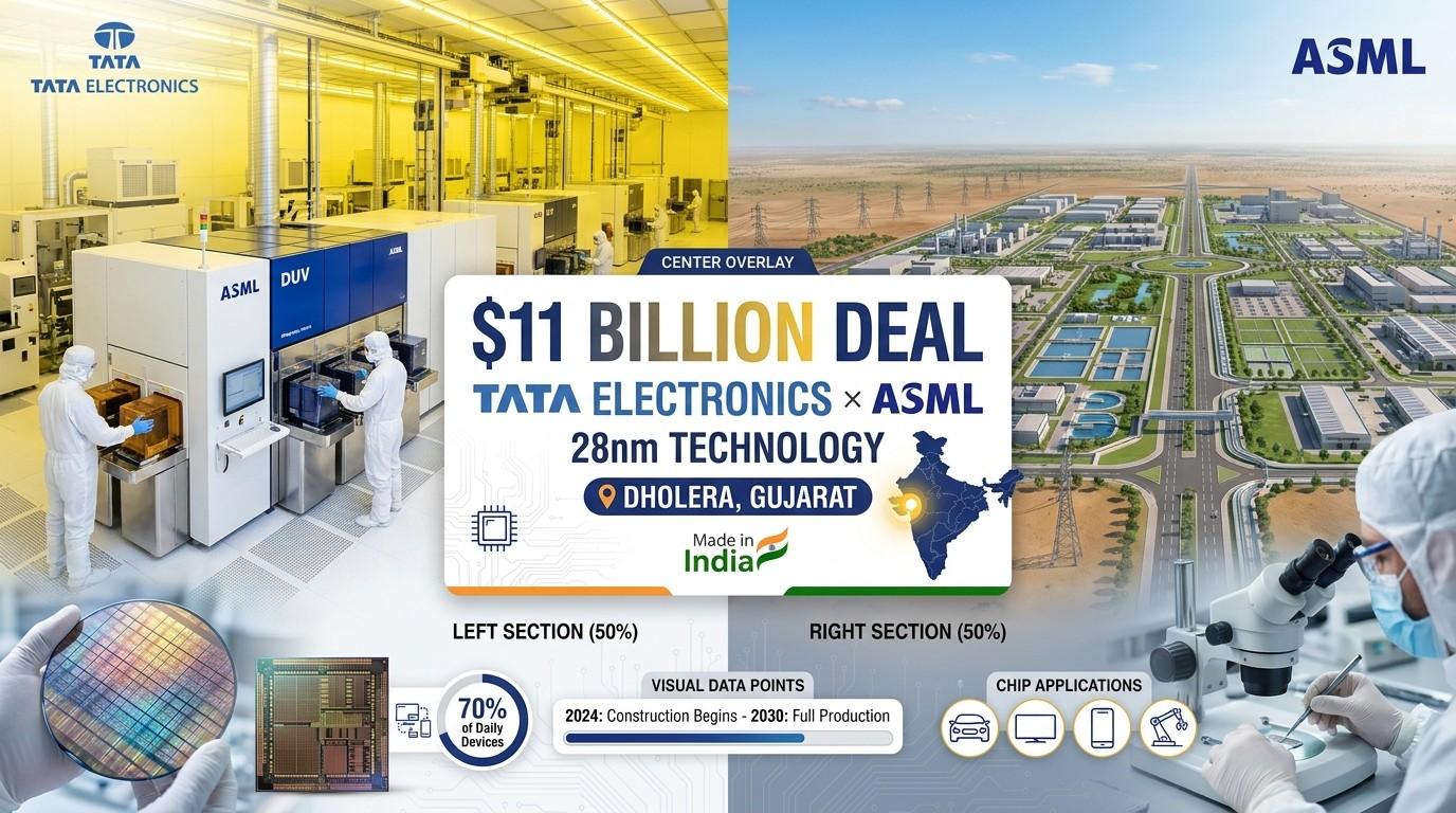
While mainstream headlines focus on cutting-edge 3nm and 2nm gate-all-around (GAA) architectures used in server CPUs and AI accelerators, mature nodes between 28nm and 14nm remain the operational backbone of the global economy. Automotive chipsets, industrial microcontrollers, baseband modems, display driver ICs, and power management modules overwhelmingly rely on mature planar and early FinFET technologies.
ASML’s TWINSCAN NXT immersion lithography systems allow Tata to achieve high wafer-per-hour (WPH) throughput with extreme overlay accuracy. By deploying deep ultraviolet light at a 193-nanometer wavelength through a water medium, these tools achieve fine resolution patterns while maintaining production stability. For Tata Electronics, mastering 28nm/22nm nodes yields three strategic advantages:
- Immediate Revenue Capture: Automotive and industrial electronics manufacturers are seeking long-term supply agreements with non-Taiwanese foundries to diversify their supply chains.
- Higher Process Stability: Mature nodes feature well-documented design rules and high base yields, minimizing initial scrap rates and lowering scrap-related capital loss.
- Pathways to Advanced Packaging: A functional front-end wafer fab enables Tata to integrate back-end testing and advanced packaging (2.5D/3D chiplets), establishing a domestic ecosystem for complex cloud compute architectures over time.
Fab Specifications and Capital Breakdown
The structural layout of the Dholera project showcases the sheer physical and operational scale required to join the global semiconductor landscape. Below is an overview of the key operational metrics and financial allocations governing the Tata-ASML project.
| Metric / Dimension | Project Specification | Strategic Significance |
|---|---|---|
| Total Estimated Outlay (CAPEX) | $11.0 Billion USD | Covers cleanroom construction, tool procurement, and site utility infrastructure. |
| Anchor Technology Partner | ASML Holding N.V. (Lithography) | Secures TWINSCAN NXT DUV Immersion Scanners & Field Engineering. |
| Initial Target Process Nodes | 28nm / 22nm planar (scaling to 14nm FinFET) | Captures high-volume automotive, power management, and industrial IoT markets. |
| Planned Wafer Capacity | 50,000 Wafer Starts Per Month (WSPM) | Achieves critical economies of scale required for unit-cost competitiveness. |
| Sovereign Fiscal Incentive (ISM 2.0) | 50% Central Grant + 20% State Co-Funding | Substantially lowers capital expenditure burdens, mitigating equity dilution risk. |
| Commercial Yield Target Date | Q4 2027 (Pilot) / Q2 2028 (Volume) | Establishes a firm timeline for commercial revenue generation and cash flow conversion. |
Industry & Market Implications: Winners, Losers, and Re-valuations
The entry of a major Indian conglomerate backed by ASML reshapes competitive dynamics across several sectors, generating distinct risk and growth profiles across equity markets.
1. Corporate Winners
Tata Group Ecosystem: Tata Motors and Tata Power gain a captive, localized semiconductor supply chain, shielding them from global chip shortages and shipping disruptions. This internal demand anchors baseline capacity utilization for TEPL, stabilizing its early cash flows.
ASML Holding N.V.: As Western geopolitical restrictions constrain ASML’s sales of mid-to-high-tier scanners in traditional markets, India emerges as a vital growth engine. This long-term equipment and service ecosystem agreement enhances ASML’s services revenue visibility.
Global Fabless Design Houses: Companies such as Qualcomm, MediaTek, and NXP Semiconductors gain a strategic secondary manufacturing base outside of East Asia, reinforcing their risk mitigation strategies.
2. The Disrupted Competition
Secondary Asian Foundries: Tier-2 and Tier-3 foundries in Taiwan, mainland China, and Southeast Asia operating in legacy nodes will face long-term margin compression. Once Tata's Dholera facility reaches volume production, price competition for mature nodes in regional markets is expected to intensify.
Frequently Asked Questions (People Also Ask)
Why did ASML choose to partner with Tata Electronics in India?
ASML's partnership with Tata Electronics addresses global demand for supply chain diversification. By supplying mature-node immersion DUV tools and technical personnel to India, ASML secures long-term tool deployments, service revenue, and a strategic position in an emerging technology ecosystem, supported by substantial state subsidies from the Indian government.
What process nodes will the Tata Dholera fab produce?
The facility will initially manufacture 28nm and 22nm node chips. These nodes are widely used in automotive control units, industrial automation systems, consumer electronics microcontrollers, and power management circuits. Over time, the facility plans to scale operations toward 14nm FinFET processes.
How does the project impact global semiconductor supply chain security?
Currently, over 70% of mature-node semiconductor capacity is concentrated in East Asia. The Tata-ASML Dholera facility establishes a secondary production center in South Asia, mitigating concentration risk stemming from potential regional conflicts, natural disasters, or trade disruptions.
What are the key execution risks facing the Tata-ASML fab?
Primary risks include building out specialized ancillary supply chains locally (such as electronic-grade gases and ultra-pure water), managing yield ramp-up timelines within a 24-to-36-month window, and continuously recruiting and retaining high-skilled lithography and process engineering talent.
Future Outlook: Execution Risks and the 2026–2030 Horizon
While the agreement between Tata and ASML provides the necessary technology and capital foundation, execution risk remains a key variable. Semiconductor fabrication facilities operate on ultra-thin margins until yield rates clear strict commercial thresholds, typically above 85% to 90% usable die per wafer.
Over the next 18 months, market analysts and institutional investors will monitor three core operational milestones:
- Utility & Cleanroom Infrastructure Delivery: The Dholera industrial zone must maintain uninterrupted power, vibration-isolated foundation slabs, and ultra-pure water filtration plants capable of processing millions of gallons daily.
- Equipment Hookup and Calibration: The arrival, uncrating, and optical alignment of ASML’s TWINSCAN NXT scanners in 2027 will test local operational readiness and engineering integration.
- Supplier Ecosystem Density: The arrival of secondary and tertiary suppliers—such as chemical suppliers, gas suppliers, and raw silicon wafer vendors—setting up shop adjacent to the Dholera site.
If Tata Electronics successfully executes its ramp-up timeline toward commercial volume production by late 2027, India will transition from a chip design hub into a full-stack semiconductor manufacturing nation. The deal with ASML delivers both the toolsets and the process discipline required to realize that goal, signaling a structural shift in how global technology infrastructure is built, capitalized, and secured for the next decade.