PUBLICATION: The Wall Street Journal, Financial Times, Bloomberg
DATE: May 6, 2021
IBM's 2nm Breakthrough: The Definitive Account of a New Era in Computing Performance and Enterprise Value
Executive Takeaways
- Historic Achievement: IBM Research has unveiled the world's first 2-nanometer (nm) node chip, produced on a 300 mm wafer, marking a pivotal advancement in semiconductor technology.
- Unprecedented Performance Gains: This new process technology promises a remarkable 45 percent performance improvement or a 75 percent reduction in power consumption compared to today's state-of-the-art 7nm chips, fundamentally altering the calculus for enterprise infrastructure scalability and operational efficiency.
- Catalyst for Key Technologies: Leveraging nanosheet technology and gate-all-around (GAA) transistors, the 2nm chip is set to unlock new frontiers in hybrid cloud architecture, artificial intelligence (AI) compute, and the Internet of Things (IoT), driving significant enterprise ROI across industries.
- R&D Leadership Reaffirmed: The breakthrough underscores IBM's enduring legacy as a foundational innovator in microelectronics, reinforcing its critical role in intellectual property development for the global semiconductor ecosystem.
Comprehensive Narrative: Engineering the Future of Compute
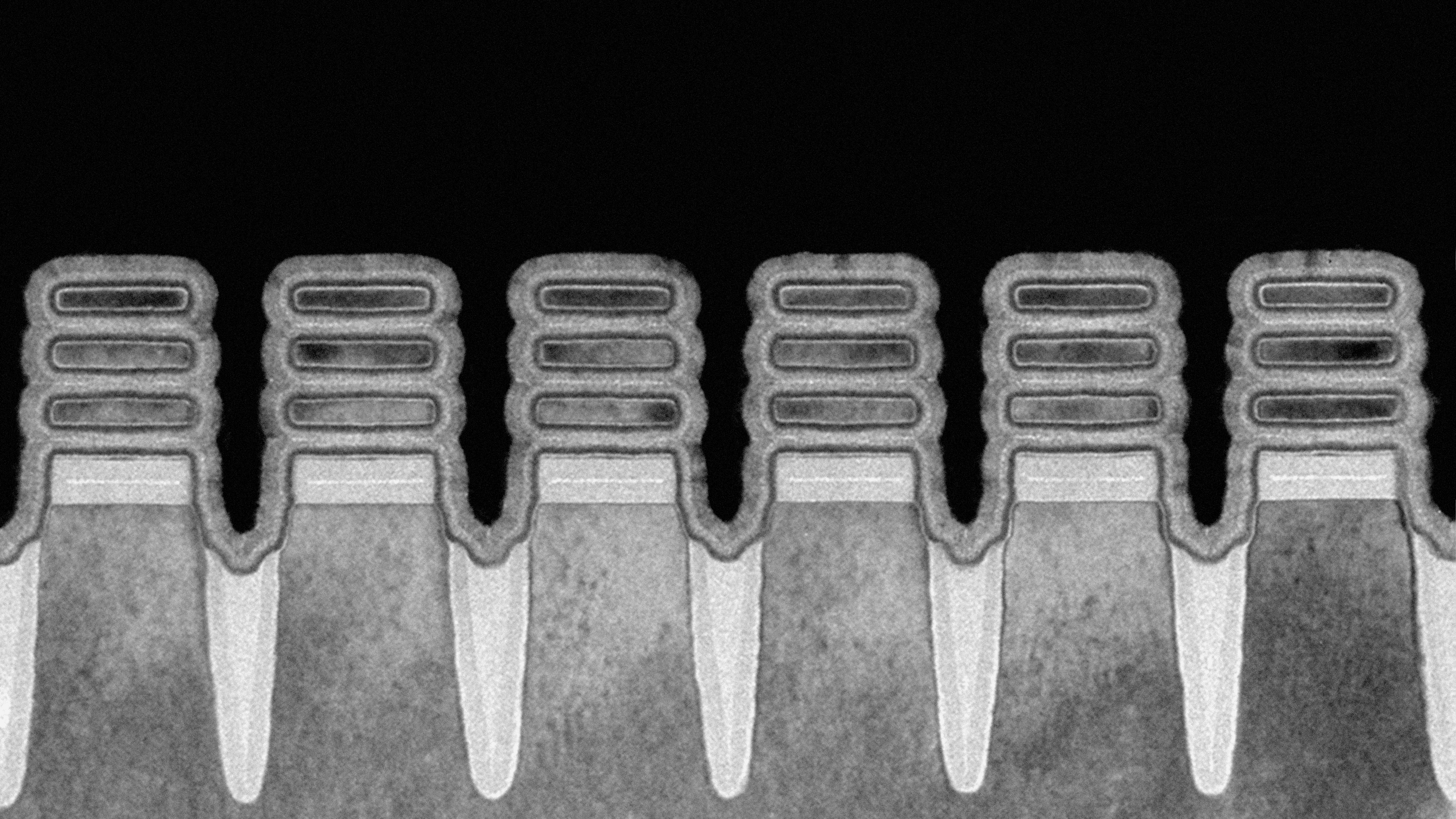
In a watershed moment for the global technology sector, IBM Research announced on May 6, 2021, the development of the world's first 2-nanometer (nm) node chip. This is not merely an incremental step but a profound leap forward, signaling a new era in semiconductor engineering that promises to redefine the boundaries of computational power, energy efficiency, and enterprise capability. Produced on a standard 300 mm wafer, this second-generation nanosheet technology test chip confirms IBM's position at the vanguard of fundamental microelectronics research, echoing its prior pioneering demonstrations of 7nm and 5nm test chips.
The relentless pursuit of Moore's Law – the exponential growth in transistor density and performance – has long driven the semiconductor industry. Yet, as physical limits loom, the engineering challenges become exponentially more complex. The transition from 7nm to 2nm represents a monumental triumph over these challenges, moving beyond the entrenched FinFET (Fin Field-Effect Transistor) architecture that has powered modern chips for over a decade. IBM's 2nm breakthrough hinges on the adoption of Gate-All-Around (GAA) transistors, built with its advanced nanosheet technology. Unlike FinFETs, which have gates on three sides of a silicon fin, GAA transistors encircle the gate entirely around the channel, providing superior electrostatic control. This enhanced control minimizes leakage current and allows for more aggressive scaling, translating directly into the reported performance and power efficiency gains.
The implications of such a leap are staggering. IBM claims its 2nm chips will deliver a 45 percent higher performance at the same power level, or conversely, consume 75 percent less power while matching the performance of contemporary 7nm chips. For enterprise clients, this dual benefit translates into critical advancements: the ability to process vastly larger datasets with reduced latency, alongside a dramatic decrease in the energy footprint of data centers. This directly impacts operational expenditure, providing a compelling pathway to improved enterprise ROI and infrastructure scalability.
This achievement is particularly timely given the escalating global demand for increased chip performance and energy efficiency. The paradigm shifts towards hybrid cloud architectures, the explosion of artificial intelligence (AI) workloads, and the pervasive expansion of the Internet of Things (IoT) have created an insatiable need for more potent, yet more frugal, silicon. AI models, for instance, are growing exponentially in complexity and size, requiring immense computational resources for training and inference. Edge AI applications, foundational to the IoT, demand powerful, low-power processing on device. IBM's 2nm technology addresses these critical requirements head-on, promising to accelerate innovation across these transformative domains.
It is important to contextualize IBM's role in this landscape. While IBM divested its chip manufacturing business to GlobalFoundries in 2015, its Research division has consistently maintained a pivotal role as an innovation engine, focusing on fundamental materials science, process technology, and architectural design. This strategy allows IBM to generate invaluable intellectual property and contribute foundational platform technology research that underpins the entire semiconductor industry. This 2nm milestone is a testament to that strategic focus, reinforcing IBM's influence as an arbiter of future technology, rather than a mass producer of chips. The patents and expertise derived from this research will undoubtedly become critical components in the licensing agreements and strategic partnerships that define the future of high-performance computing.
Verified Data / Metrics Breakdown
The table below illustrates the profound generational leap represented by IBM's 2nm test chip compared to prevalent 7nm technology at the time of its announcement.
| Feature / Metric | State-of-the-Art 7nm (Production 2021) | IBM 2nm Test Chip (Announced May 2021) |
|---|---|---|
| Process Node | 7 nm | 2 nm |
| Key Transistor Architecture | FinFET (Fin Field-Effect Transistor) | GAA (Gate-All-Around) Nanosheet |
| Performance Improvement (vs. 7nm) | Baseline | Up to 45% Higher Performance |
| Power Consumption Reduction (vs. 7nm) | Baseline | Up to 75% Lower Power |
| Wafer Size | Typically 300 mm | 300 mm |
| Primary Driver for Scaling | Geometric scaling, improved FinFETs | Enhanced electrostatic control via GAA |
Industry & Market Implications: Reshaping the Global Tech Landscape
The ripple effects of IBM's 2nm announcement are poised to transform numerous sectors, influencing everything from capital allocation strategies to long-term valuation multiples for technology enterprises.
Who Wins?
- Cloud Service Providers (CSPs): Hyperscalers like AWS, Azure, and Google Cloud stand to gain immensely. With 2nm chips, they can achieve unprecedented infrastructure scalability, packing more compute power into existing data center footprints while drastically reducing energy consumption and cooling costs. This directly translates to enhanced profit margins and superior service offerings, critical for maintaining competitive advantage and attracting high-value enterprise clients.
- Enterprise Technology Buyers: Organizations heavily reliant on data processing – financial institutions, healthcare providers, manufacturing firms – will see significant improvements in operational efficiency and speed. Faster transaction processing, real-time analytics, sophisticated risk mitigation models, and accelerated drug discovery simulations become more economically viable, directly impacting enterprise ROI.
- AI and Machine Learning Innovators: The sheer compute density of 2nm chips will empower the development of more complex, higher-fidelity AI models, both at the data center and the edge. This fuels breakthroughs in areas like natural language processing, computer vision, and autonomous systems, creating new market liquidity and investment opportunities.
- IBM and its Partners: IBM solidifies its intellectual property portfolio and leadership in fundamental research, positioning itself as a crucial enabler for foundry partners like Samsung and TSMC, who will ultimately commercialize these process technologies. This enhances IBM's strategic relevance and potential for licensing revenue.
- Consumers: While indirect, the benefits will eventually filter down to consumer electronics, leading to smartphones with significantly longer battery life, more powerful laptops, and smarter IoT devices.
Who Faces Challenges?
- Semiconductor Competitors: Companies like Intel, still catching up on leading-edge process nodes, face intensified pressure to accelerate their R&D and manufacturing roadmaps. The capital expenditure required to keep pace with these advancements is staggering, impacting future earnings and market share.
- Supply Chain Concentration: As fewer companies possess the capabilities for advanced node manufacturing, the global semiconductor supply chain could become even more concentrated, raising concerns about geopolitical risks, regulatory compliance, and resilience.
- Legacy Infrastructure Providers: Enterprises unable or unwilling to upgrade their compute infrastructure face increasing competitive disadvantage due to higher operational costs and lower performance ceilings compared to those leveraging advanced silicon.
Economically, this breakthrough represents a powerful deflationary force for compute power, enabling more for less. It accelerates the digital transformation across all industries, driving productivity gains and fostering innovation. The strategic implications extend to national security and global technological leadership, as the race for semiconductor supremacy intensifies.
People Also Ask (FAQ)
What exactly is a 2nm chip, and how does it compare to current technology?
A 2nm chip refers to the "2-nanometer node" in semiconductor manufacturing, indicating a significant reduction in the size of individual transistors and the spacing between them. While "nm" has evolved from a direct measure of physical gate length to a marketing term for a generation of technology, it signifies a dramatically increased transistor density. Compared to the 7nm chips prevalent in high-end devices and data centers in 2021, IBM's 2nm test chip promises a 45% increase in performance at the same power level, or a 75% reduction in power consumption for equivalent performance. This means exponentially more processing power can be packed into the same physical space, or existing compute tasks can be performed with far greater energy efficiency.
What is "nanosheet" and "gate-all-around" technology, and why is it crucial for 2nm?
"Nanosheet" and "Gate-All-Around" (GAA) are foundational technologies enabling the 2nm node. For decades, chips relied on planar transistors, then transitioned to FinFETs (Fin Field-Effect Transistors) for nodes like 22nm, 14nm, 7nm, and 5nm. FinFETs offer improved electrostatic control by wrapping the gate around three sides of a silicon "fin." However, as transistors shrink further, FinFETs reach their physical limits in managing leakage currents. GAA transistors overcome this by completely encircling the channel (a nanosheet, which is essentially a very thin, stacked layer of silicon) with the gate material. This "gate-all-around" design provides superior electrostatic control, minimizing leakage, improving power efficiency, and enabling the continued scaling necessary for 2nm and beyond. IBM's nanosheet technology optimizes the design and stacking of these channels.
How will IBM's 2nm chip impact enterprise computing, hybrid cloud, and AI?
The impact will be transformative across enterprise computing, hybrid cloud, and AI. For enterprise computing, 2nm chips will enable vastly faster data processing for complex applications like financial modeling, scientific simulations, and real-time business intelligence, boosting enterprise ROI. In hybrid cloud environments, the ability to pack more computational power into server racks while significantly reducing power consumption will lead to massive infrastructure scalability, lower operational costs, and reduced carbon footprints for data centers. For AI, the increased transistor density and energy efficiency will accelerate the training of larger, more sophisticated neural networks, facilitate the deployment of powerful AI models at the edge (e.g., in autonomous vehicles or IoT devices), and drive breakthroughs in machine learning capabilities across all industries.
Will IBM manufacture these chips, or who will?
While IBM Research developed the 2nm test chip, IBM itself is not a mass manufacturer of advanced semiconductors. IBM's role is primarily in fundamental research, intellectual property development, and process technology innovation. The commercial manufacturing of these 2nm chips will likely be handled by leading global foundries such as TSMC, Samsung Foundry, or potentially Intel Foundry Services, through strategic partnerships and licensing agreements with IBM. These foundries possess the immense capital, infrastructure, and specialized expertise required for high-volume, cutting-edge semiconductor fabrication. IBM's breakthrough provides the foundational technology and blueprint for these manufacturing giants to license and implement in their future production lines.
Future Outlook: The Road Ahead for Atomic-Scale Engineering
The announcement of the 2nm chip, while groundbreaking, is but a waypoint on the relentless march of semiconductor innovation. The transition from a test chip to mass production is a complex, multi-year endeavor, typically involving billions of dollars in capital allocation for new fabrication facilities, extensive validation, and yield optimization. Industry analysts project that the first commercial products leveraging 2nm technology could emerge in the 2024-2025 timeframe, depending on the speed of foundry partners' adoption and scaling.
The challenges are substantial: perfecting manufacturing processes at atomic scales, managing increasing design complexity, mitigating quantum effects, and controlling escalating production costs. However, the economic impetus for higher performance and lower power consumption remains immense. This breakthrough reaffirms the importance of sustained, high-value R&D investment and collaborative ecosystems between research institutions and manufacturing giants. Beyond 2nm, the industry's gaze is already fixed on 1nm and the frontiers of materials science, exploring new transistor architectures, novel materials, and even quantum computing paradigms. IBM's 2nm achievement not only pushes the current boundaries of silicon but also lays critical groundwork for the next generation of computing, shaping the strategic landscape for decades to come.