Inside India’s $15 Billion Chip Rush: The Complete 2026 Registry of Silicon Fabs, Compound Plants, and OSAT Facilities
By the Global Technology & Markets Desk | Special Investigative Report
Published: August 17, 2026, 16:01 IST | Updated for Institutional Investors
Executive Takeaways
- Strategic Industrial Shift: India's semiconductor manufacturing ecosystem has officially transitioned from policy aspiration to active physical infrastructure in 2026, backed by a multi-billion dollar capital allocation strategy.
- Current Project Breakdown: The national footprint currently comprises 1 primary silicon fabrication facility, 2 compound semiconductor plants, and multiple outsourced semiconductor assembly and test (OSAT) units.
- Global Supply Chain Realignment: International joint ventures spanning the US, Japan, Taiwan, and domestic conglomerates are fundamentally mitigating single-source geopolitical risk for multinational technology enterprises.
- Enterprise ROI & Valuation Horizons: Investors are evaluating infrastructure scalability, regulatory compliance frameworks, and long-term market liquidity as these facilities approach initial wafer tape-outs.
The Geopolitical and Economic Imperative Behind India's Silicon Ascent
For decades, global electronics manufacturing faced a precarious structural bottleneck: extreme geographic concentration of semiconductor fabrication. As geopolitical tensions mounted and supply chain vulnerabilities crippled automotive, consumer electronics, and enterprise server markets, global conglomerates initiated aggressive risk mitigation protocols. Amid this worldwide scramble for supply chain diversification, India has emerged as a formidable focal point. By mid-2026, the subcontinent’s semiconductor landscape has shifted decisively from memorandum-of-understanding announcements to tangible steel, concrete, and cleanroom installations.
Propelled by the modified Semicon India Programme—which offers substantial fiscal support covering up to 50% of project capital expenditure—state and central authorities have successfully courted tier-one technology titans and foundry operators. This capital allocation is not merely an exercise in industrial self-reliance; it is a calculated bid to capture high-margin segments of the global technology value chain. Institutional investors tracking valuation multiples in semiconductor capital equipment, specialty chemicals, and cloud compute architecture are now aggressively recalibrating their portfolios to factor in India’s domestic manufacturing footprint.
Decoding the 2026 Plant Topology: Fabs, Compound Semiconductors, and OSATs
A granular examination of the verified project registry reveals a carefully diversified operational matrix. Unlike historical missteps where policymakers chased bleeding-edge sub-2-nanometer nodes prematurely, the current strategy focuses on high-demand, high-utility nodes (ranging from mature 28nm to 90nm legacy architectures) alongside advanced packaging and compound semiconductors essential for electric vehicles (EVs), telecommunications, and power electronics.
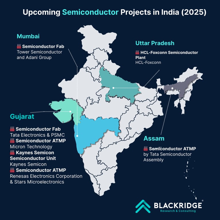
The current active roster includes 1 primary silicon fabrication facility designed for high-volume CMOS logic and analog wafers, supplemented by 2 specialized compound semiconductor manufacturing plants focusing on wide-bandgap materials like Gallium Nitride (GaN) and Silicon Carbide (SiC). Furthermore, a robust network of Outsourced Semiconductor Assembly and Test (OSAT) and Advanced Packaging facilities is anchoring the back-end processing pipeline across states like Gujarat, Assam, and Tamil Nadu.
Verified Data Registry: Semiconductor Plants in India (2026 Status)

The following institutional-grade matrix details the authorized semiconductor facilities, their geographical locations, technology nodes, and strategic partner alignments as tracked by market intelligence sources in August 2026.
| Facility Type | Location | Key Partners / Promoters | Node / Technology Focus | Estimated Outlay / Status (2026) |
|---|---|---|---|---|
| Silicon Fab (Logic/Analog) | Dholera, Gujarat | Tata Electronics & PSMC (Taiwan) | 28nm, 40nm, 55nm, 90nm | ~$11 Billion | Construction & Tool In-flow Phase |
| Compound Semiconductor | Mysuru, Karnataka | RPi Semiconductor | Silicon Carbide (SiC) / GaN Power Diodes | ~$400 Million | Pilot Production Scaling |
| Compound Semiconductor / OSAT | Sanand, Gujarat | CG Power, Renesas, & Stars Microelectronics | OSAT, Power Discretes, RF Components | ~$1.05 Billion | Infrastructure Fit-out |
| Advanced OSAT Facility | Morigaon, Assam | Tata Electronics Private Limited | Flip Chip & Wire Bond Packaging | ~$3.27 Billion | Active Workforce Training & Rollout |
Industry & Market Implications: Winners, Losers, and Macro Economics
The operationalization of these semiconductor assets reshapes the competitive dynamics for regional and global market participants.
- The Winners: Domestic industrial conglomerates, specialized EPC (Engineering, Procurement, and Construction) firms, and international equipment manufacturers (such as photolithography and deposition vendors) are seeing record order books. Automotive OEMs and consumer electronics brands operating within South Asia secure a localized, tariff-mitigated supply chain.
- The Losers: Legacy export hubs that failed to diversify their regional packaging footprint face margin compression. Furthermore, domestic electronic system design and manufacturing (ESDM) firms that previously relied exclusively on 100% imported silicon must rapidly adapt their procurement contracts to leverage domestic foundry quotas.
- Macroeconomic Impact: Beyond trade deficit adjustments, the spillover effect into high-end talent acquisition, intellectual property creation, and cleanroom engineering standards establishes a permanent structural upgrade for India’s industrial base.
Frequently Asked Questions (People Also Ask)
Q: How many total semiconductor manufacturing units are currently approved or operational in India as of 2026?
As of August 2026, the central government has formally approved and backed several major semiconductor projects. This includes 1 primary silicon wafer fabrication plant (Dholera), 2 compound semiconductor manufacturing facilities (including Mysuru and Sanand alignments), and multiple advanced OSAT (Outsourced Semiconductor Assembly and Test) facilities, representing a cumulative committed investment exceeding $15 billion.
Q: What specific technology nodes are being prioritized by Indian semiconductor fabs?
Rather than attempting to immediately manufacture bleeding-edge sub-2nm nodes, Indian facilities are strategically prioritizing high-demand mature and legacy nodes—specifically 28nm, 40nm, 55nm, and 90nm processes. These nodes power the vast majority of automotive systems, industrial automation, power management ICs, consumer appliances, and IoT devices.
Q: Which international technology partners are collaborating with Indian firms on these projects?
Major domestic conglomerates like Tata Electronics have partnered with global heavyweights such as Taiwan’s Powerchip Semiconductor Manufacturing Corporation (PSMC). Other ventures incorporate collaborations with Japanese tech giants like Renesas Electronics and global packaging specialists like Stars Microelectronics to ensure technical viability and process transfer.
Q: What are the primary economic and risk factors influencing enterprise investment in these facilities?
Key institutional considerations include infrastructure scalability (reliable ultra-pure water and uninterrupted power supply), regulatory compliance and subsidy disbursement speeds, long-term market liquidity, and talent pipeline maturation. Investors closely monitor cleanroom construction milestones and initial commercial tape-out schedules to gauge enterprise ROI.
Future Outlook: Milestones and Catalysts to Watch Through 2030
As the calendar advances toward the end of the decade, the litmus test for India’s semiconductor strategy will transition from capital deployment to commercial yield efficiency and volume scaling. Key milestones to monitor include the first commercial wafer tape-outs from the Dholera silicon fab expected late in the cycle, the integration of local compound semiconductor output into domestic electric vehicle manufacturing lines, and the expansion of secondary supplier ecosystems providing specialty gases, photoresists, and ultra-pure chemicals locally.
For institutional investors, private equity syndicates, and corporate strategists, maintaining rigorous oversight of regulatory adjustments, operational risk mitigation, and technological yield reports will remain critical as India firmly embeds itself into the architecture of global semiconductor manufacturing.