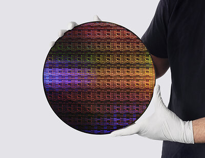
NEW YORK — In a move that redraws the global geopolitical and technological roadmap, IBM has shattered the theoretical limits of silicon semiconductor engineering. Announcing from its Albany Nanotech Complex, the computing giant has debuted the world’s first sub-1 nanometer (nm) chip technology.
By leveraging a radical, newly patented "nanostack" 3D chip architecture, IBM has successfully packed nearly 100 billion transistors onto a single slice of silicon no larger than a human fingernail. The breakthrough arrives at a critical juncture, as the global buildout of artificial intelligence threatens to outstrip the world's energy grids, making extreme chip efficiency the ultimate currency of the modern tech economy.
For decades, physicists and semiconductor executives warned of an impending "brick wall" where physical limitations would prevent transistors from shrinking further. With this announcement, IBM has not only bypassed that wall; it has built a new vertical highway directly over it.
The Physics of the Breakthrough: What is 'Nanostack' 3D Architecture?
Historically, chip scaling progressed horizontally. Manufacturers squeezed more transistors onto a flat plane. When that hit physical limits, the industry transitioned to nanosheets. IBM’s new sub-1 nm technology takes this concept into the third dimension with its proprietary "Nanostack" 3D architecture.
Instead of placing transistor channels side-by-side, IBM’s engineers have vertically stacked multiple active silicon nanosheet layers on top of one another within a sub-1nm gate pitch. This vertical integration reduces the distance signals must travel, slashes resistance, and minimizes heat generation.
Key Architectural Innovations:
- Vertical Nanosheet Stacking: Maximizes the drive current per unit of footprint by stacking up to six nanosheet channels vertically.
- High-k Metal Gate (HKMG) Evolution: Utilizes novel atomic-layer deposition techniques to prevent quantum tunneling—a phenomenon where electrons leak through barriers that are too thin.
- Backside Power Delivery: Separates the power distribution network from the signal-carrying metal layers, placing it on the underside of the wafer to reduce voltage drop and boost efficiency.
Why It Matters: The Solution to AI’s Insatiable Energy Appetite

The timing of IBM’s breakthrough is as strategic as the technology itself. Generative AI applications, high-performance computing (HPC), and massive LLM (Large Language Model) training runs are consuming unprecedented amounts of electricity. According to recent energy forecasts, data center power demands are projected to triple by 2030.
IBM estimates that its sub-1 nm architecture could unlock a staggering 75% reduction in power consumption compared to today’s leading-edge 3nm chips, while maintaining identical performance levels. Alternatively, for high-compute workloads, the technology can deliver a 50% performance leap within the same power envelope.
For hyperscalers like Microsoft, Google, and Meta, implementing this technology at scale could save billions of dollars in utility costs and significantly reduce the carbon footprint of global data centers.
How Sub-1nm Compares to Current Frontiers
To understand the sheer scale of IBM’s achievement, it is useful to compare this new technology against current-generation production nodes and near-future roadmaps:
| Metric / Feature | Current Leading-Edge (3nm Class) | Upcoming Horizon (2nm Class) | IBM Sub-1nm Technology |
|---|---|---|---|
| Transistor Density | ~150–200 Million / mm² | ~250��310 Million / mm² | ~650+ Million / mm² |
| Primary Architecture | FinFET / Early Nanosheet | GAA (Gate-All-Around) Nanosheet | 3D "Nanostack" GAA |
| Power Reduction (vs. 3nm) | Baseline | ~25-30% Reduction | ~75% Reduction |
| Performance Gain (vs. 3nm) | Baseline | ~15-20% Increase | ~50% Increase |
| Primary Application Target | Mobile, Consumer CPUs | Next-Gen Servers, Mobile Chips | Hyperscale AI, Quantum & Supercomputing |
Geopolitical Implications and the Race to Commercialization
IBM operates on a fabless model for commercial production, meaning it designs and prototypes these revolutionary nodes at its state-of-the-art Albany facility, but relies on manufacturing partners to bring them to market. Historically, IBM has partnered with Samsung and Intel, while also licensing intellectual property to Japan’s state-backed foundry startup, Rapidus.
This sub-1 nm breakthrough fires a direct shot across the bow of TSMC, the world’s undisputed foundry king, which is currently racing toward its own "A16" (1.6nm) and "A14" (1.4nm) processes scheduled for late 2026 and 2028 respectively. By proving the viability of sub-1nm silicon ahead of its rivals, IBM secures an invaluable intellectual property moat.
"This isn't just an incremental step; it's a paradigm shift," said an industry analyst close to the Albany project. "IBM has shown the world that silicon still has a long life ahead of it. The focus now shifts to who can yield this architecture at scale first."
Looking Ahead: When Will Sub-1nm Enter the Market?
While the laboratory demonstration is a historic triumph, consumers and enterprise buyers will need to exercise patience. Translating a lab-proven sub-1nm prototype into high-yield, high-volume manufacturing is a notoriously difficult engineering challenge.
Industry insiders expect IBM’s licensing partners to integrate elements of this 3D Nanostack technology into commercial foundry roadmaps by late 2029 or early 2030. Between now and then, the industry must perfect Extreme Ultraviolet (EUV) lithography systems with higher numerical apertures (High-NA EUV) capable of etching features at this atomic scale.
Nevertheless, the message from IBM is loud and clear: the silicon age is far from over, and the race to dominate the foundations of artificial intelligence has entered its most intense chapter yet.
Frequently Asked Questions
1. Is the sub-1nm chip ready for commercial use?
No. Currently, this is a pioneering technology demonstration and functional prototype developed at IBM's Albany research facility. The technology must now undergo rigorous manufacturing optimization with foundry partners (such as Samsung, Intel, or Rapidus) before entering commercial production, which is projected to begin around 2029–2030.
2. How does IBM pack 100 billion transistors onto such a small space?
By moving from a 2D horizontal layout to a 3D "Nanostack" architecture. Instead of placing transistors next to each other on the flat plane of the silicon wafer, IBM stacks up to six nanosheet channels vertically on top of each other. This vertical architecture utilizes the Z-axis, drastically increasing density without increasing the physical footprint of the chip.