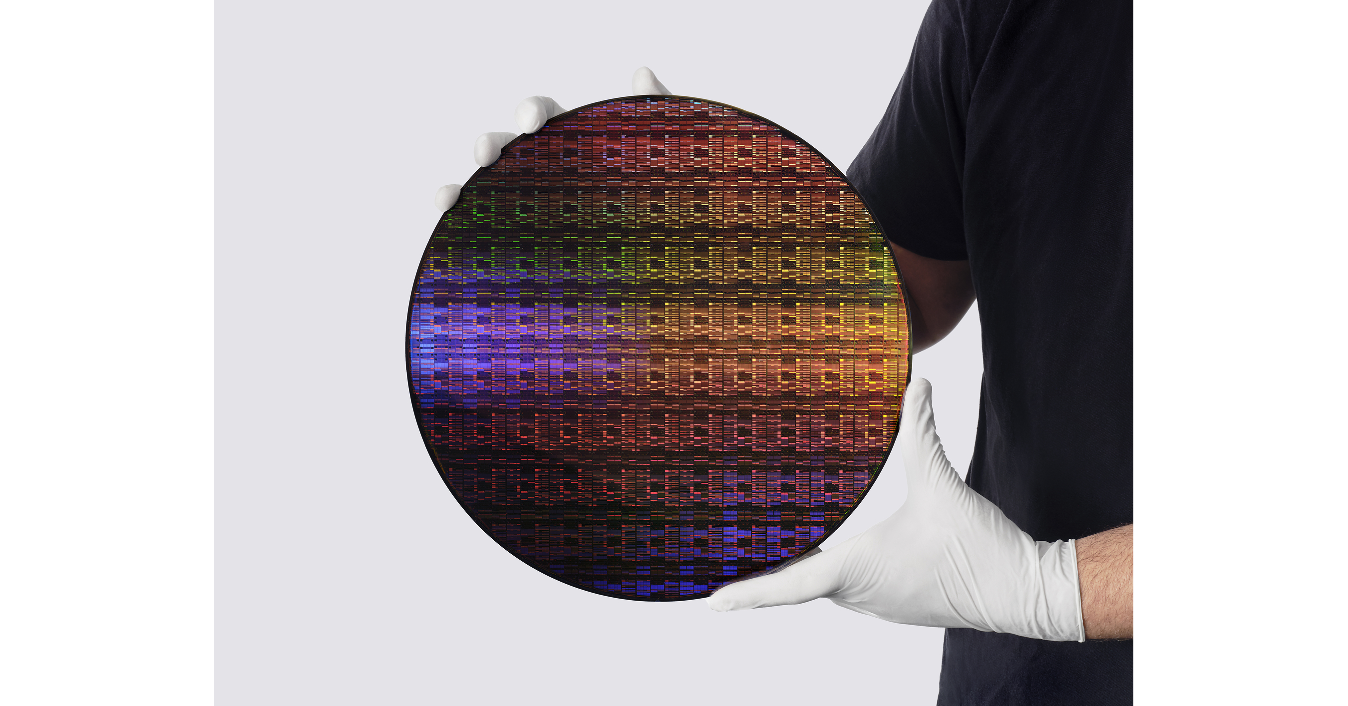
NEW YORK & BENGALURU — In a move that effectively rewrites the laws of semiconductor physics and redraws the geopolitical map of high-tech manufacturing, IBM has officially debuted the world’s first sub-1 nanometer (nm) chip technology. The historic breakthrough, announced via the IBM Newsroom on June 25, 2026, promises to unlock unprecedented computing speeds while dramatically slashing the carbon and energy footprint of the global artificial intelligence boom.
For decades, the semiconductor industry has chased the elusive limits of Moore’s Law—the observation that the number of transistors on a microchip doubles roughly every two years. As silicon transistors approached atomic scales, many feared that quantum tunneling and thermal dissipation would bring this progression to a grinding halt. IBM’s latest achievement proves those skeptics wrong, leveraging a radically new architecture to pack an astronomical number of switches onto a sliver of silicon no larger than a human fingernail.
The ‘Nanostack’ Breakthrough: How IBM Shrunk the Unshrinkable
At the heart of this milestone is IBM’s proprietary “nanostack” 3D chip architecture. Traditional chips place transistors side-by-side in a two-dimensional plane. While previous innovations like nanosheet technology (pioneered by IBM in its 2021 2nm announcement) allowed gates to wrap around channels, they still faced physical horizontal limits.
The sub-1nm design bypasses these limits by vertically stacking active transistor channels in a highly synchronized, multi-layered 3D matrix. This structural shift allows IBM to pack nearly 100 billion transistors onto a single, fingernail-sized chip. By utilizing advanced Extreme Ultraviolet (EUV) lithography techniques alongside novel material composition, engineers have minimized resistance and leakage at the atomic level.
“IBM’s latest chip breakthrough marks a landmark moment in semiconductor history,” noted a senior technology strategist familiar with the development. “By mastering sub-1nm architecture, they aren’t just iterating; they are introducing a fundamentally new dimension to how computers process data. This is the bridge to the post-silicon era.”
Key Specifications: Comparing the Generations

To put this milestone into perspective, the table below highlights how IBM’s sub-1nm technology compares to its previous industry-leading 2nm node, illustrating the dramatic leap in density and operational efficiency:
| Metric / Attribute | IBM 2nm Node (2021) | IBM Sub-1nm Breakthrough (2026) |
|---|---|---|
| Transistor Count (Fingernail Size) | 50 Billion | Nearly 100 Billion |
| Core Architecture | Horizontal Nanosheet (GAA) | 3D "Nanostack" Architecture |
| Expected Power Reduction | Up to 75% vs. 7nm | Up to 85% vs. 2nm equivalent processes |
| Target Market Applications | Mobile, Cloud Hyperscalers | Generative AI, Quantum-Hybrid systems, Edge HPC |
Solving the AI Energy Crisis
The timing of IBM’s breakthrough could not be more critical. The meteoric rise of generative AI models, large-scale LLMs (Large Language Models), and autonomous systems has triggered an unprecedented global energy crisis. Data centers worldwide are consuming power at rates that threaten municipal grids, with thermal management and electricity sourcing becoming the primary bottlenecks for AI progress.
By shrinking the architecture to a sub-1nm scale, IBM addresses this challenge head-on. The shortened physical distance between transistors minimizes electron travel time and drastically reduces resistance-generated heat. Key benefits of this power-efficiency curve include:
- Decarbonizing Hyperscale Data Centers: Replacing current-generation enterprise chips with sub-1nm equivalents could save billions of kilowatt-hours annually, potentially offsetting millions of metric tons of CO2 emissions.
- Prolonging Battery Life: For mobile, IoT, and edge devices, the architecture could slash power consumption, allowing smartphones to maintain multi-day battery lives even while running complex on-device AI models.
- Enhanced Thermal Performance: Cooler operation means data centers require less mechanical cooling infrastructure, driving down both capital expenditure (CapEx) and operational expenditure (OpEx).
The Foundry Race: Commercializing the Technology
While IBM continues to lead the world in fundamental semiconductor research, the company operates as a fabless developer for its commercial chips. This means the race is now on among global foundries to license and manufacture this sub-1nm blueprint.
Industry analysts point to IBM's historic manufacturing partners, such as Samsung Electronics and Rapidus in Japan, as the logical frontrunners to pilot this technology. Meanwhile, competitors like TSMC and Intel are working on their own proprietary Angstrom-era nodes (such as TSMC's A16 and Intel's 14A processes). IBM's sub-1nm announcement leapfrogs these timelines, placing immense pressure on the rest of the supply chain to match their physical design capabilities.
Commercial deployment, however, will not happen overnight. Transitioning from a functional research laboratory prototype to mass wafer yields requires fine-tuning High-NA EUV lithography machines and mastering the deposition of raw materials at an atomic-layer thickness of just a few angstroms. Industry insiders expect initial commercial applications of the sub-1nm technology to debut in specialized enterprise clouds and supercomputing facilities by late 2029.
Frequently Asked Questions
What exactly does "sub-1 nanometer" mean in chip design?
In modern semiconductor engineering, the term "nanometer" no longer refers to the physical gate length of a transistor, but rather serves as a marketing and structural generation indicator. A "sub-1 nanometer" chip means the structural features, gate pitches, and atomic-scale stacking configurations are equivalent to scaling thresholds below 10 angstroms (1 nanometer = 10 angstroms), enabling unprecedented transistor density and efficiency.
How does the "nanostack" 3D design help reduce power?
Traditional flat chips suffer from "parasitic capacitance" and electron leakage when transistors are shrunk too close to one another on a 2D plane. IBM’s "nanostack" architecture stacks the components vertically. This allows the electrical currents to be controlled precisely on three dimensions with minimized physical distance, drastically reducing resistance, heat output, and the overall electrical energy required to switch states.