Executive Takeaways
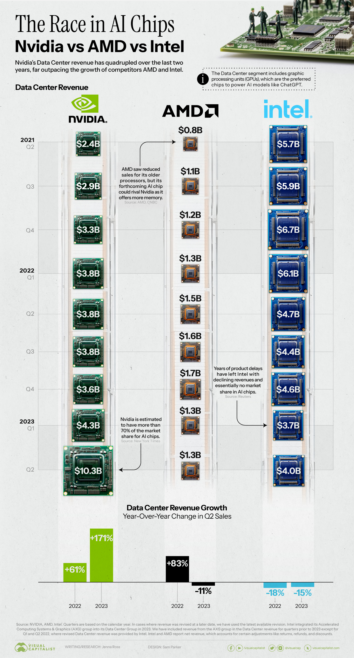
- Nvidia’s Fortified Moat Under Siege: While Nvidia commands roughly 80% to 90% of the data center AI acceleration market, a coalition of hyperscalers, legacy semiconductor giants, and venture-backed startups are deploying over $100 billion in research and development to dismantle its CUDA software lock-in and high-margin pricing power.
- The Custom Silicon Pivot: Big Tech hyperscalers—led by Google, Amazon, Microsoft, and Meta—are aggressively transitioning from merchant silicon buyers to bespoke Application-Specific Integrated Circuit (ASIC) designers, seeking to compress operational expenditures and mitigate supply-chain vulnerability.
- Architectural Diversification: Beyond traditional GPUs, alternative architectures including Linear Processing Units (LPUs), spatial dataflow processors, wafer-scale engines, and photonic interconnects are redefining inference latency, addressing the physics of the "memory wall."
- Capital Allocation Crossroads: Enterprise return on investment (ROI) is replacing raw compute performance as the industry’s north-star metric, shifting procurement criteria toward Total Cost of Ownership (TCO), energy efficiency per watt, and open-source software interoperability.
The High-Stakes Geopolitics of Parallel Computing
In the subterranean cleanrooms of Hsinchu, Oregon, and Dresden, the architecture of the modern global economy is being cast in silicon. Compute capacity has decoupled from traditional enterprise IT budgeting to become the foundational asset of global gross domestic product. What began as a computational breakthrough in deep learning has mutated into an industrial arms race where capital allocation, sovereign industrial policy, and computational physics collide.
For decades, semiconductor design prioritized general-purpose scalar execution, anchored by the x86 architecture of Intel and AMD. Today, generative artificial intelligence, multi-modal foundation models, and sovereign inference engines demand unprecedented parallel computing capabilities. As a result, the global semiconductor market is bifurcating between commodity components and high-margin, highly specialized AI accelerators designed to process trillions of matrix math calculations per second.
At the apex of this commercial tectonic shift sits Nvidia Corporation. By coupling its proprietary Tensor Core architecture with the CUDA (Compute Unified Device Architecture) software ecosystem over an eighteen-year horizon, Nvidia achieved a near-monopolistic stranglehold on accelerated data center computing. However, as enterprise procurement teams face astronomical prices, protracted lead times, and structural gross margins exceeding 75% for Nvidia’s flagship silicon, a comprehensive counter-offensive has materialized across the global technology ecosystem.
Mapping the 30+ Players Reshaping the AI Chip Landscape
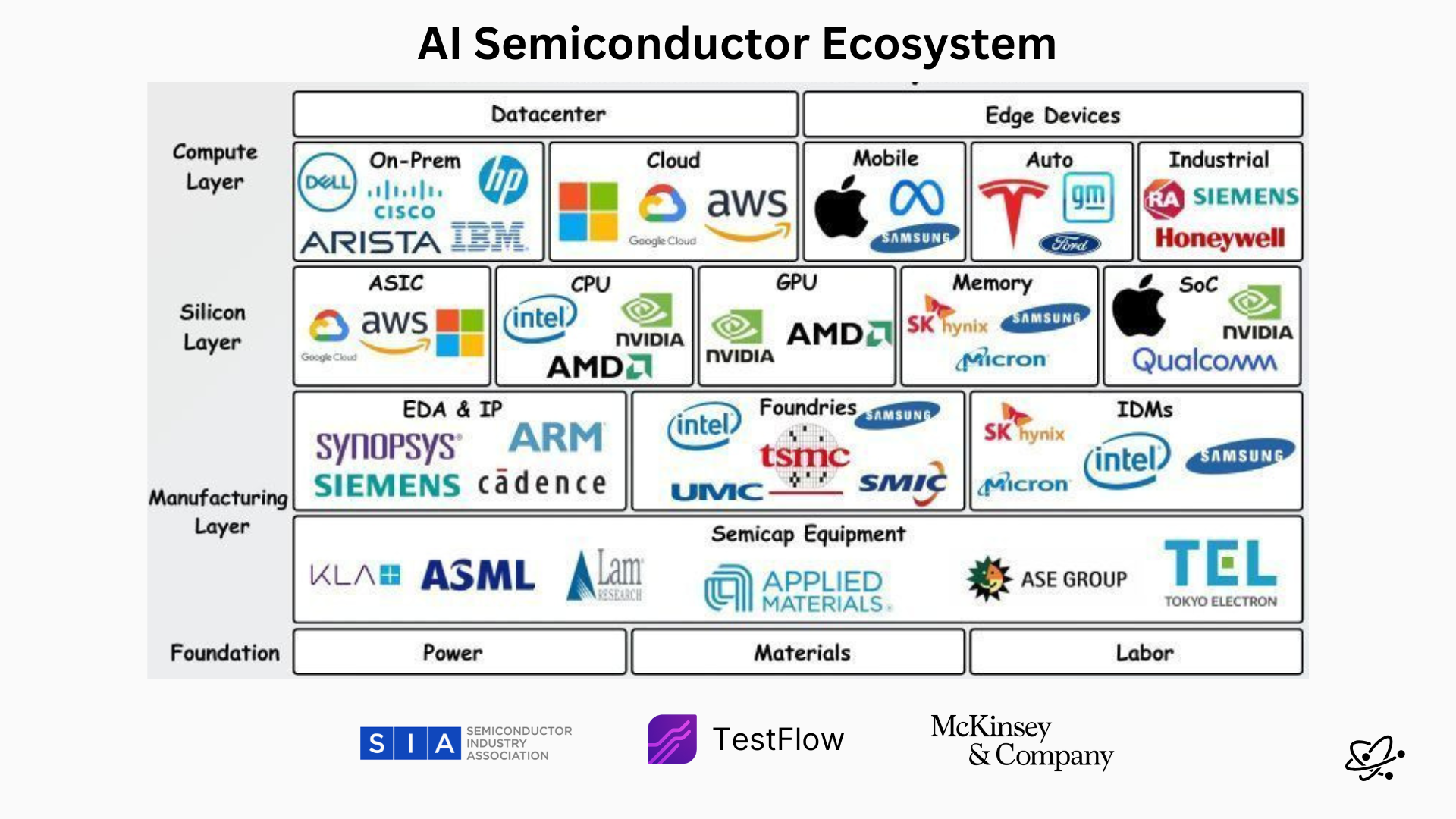
The global AI semiconductor landscape now spans far beyond conventional merchant silicon providers. It comprises a complex matrix of sovereign foundries, hyperscale cloud service providers (CSPs), legacy integrated device manufacturers (IDMs), and specialized pure-play innovators targeting discrete points along the training and inference pipeline.
1. The Merchant Silicon Incumbents
The core enterprise compute layer remains a battleground among the traditional semiconductor titans seeking broad merchant distribution across Tier-1 enterprise and cloud environments.
- Nvidia: The undisputed market sovereign, extending its lead with the Blackwell B200 and GB200 NVL72 architectures, combining dual-die packaging, second-generation transformer engines, and extreme interconnect bandwidth.
- Advanced Micro Devices (AMD): Nvidia’s most credible merchant challenger. The Instinct MI300X and MI325X platforms, powered by the open-source ROCm software stack, utilize CDNA 3 chiplet architectures and industry-leading High Bandwidth Memory (HBM3e) capacities to challenge Nvidia on enterprise TCO.
- Intel: Reorienting its enterprise strategy around the Gaudi 3 accelerator, focusing aggressively on price-to-performance efficiency and native Ethernet scalability to counter proprietary fabric lock-ins.
2. The Hyperscale Custom ASIC Vanguard
Tired of subsidizing Nvidia’s hardware margins, the world’s largest cloud infrastructure operators are designing custom silicon to insource compute and lock enterprise clients into their respective cloud fabrics.
- Google (Alphabet): The pioneer of custom silicon, deploying its 6th-generation Tensor Processing Unit (TPU v6e / Trillium) to power internal search, Gemini model training, and external Google Cloud Platform (GCP) enterprise workloads.
- Amazon Web Services (AWS): Driving margin optimization via Trainium2 for deep model training and Inferentia2 for low-cost token generation, integrated directly into the AWS EC2 virtualization architecture.
- Microsoft: Deploying the Azure Maia 100 accelerator alongside cobalt CPUs, designed explicitly to power Azure OpenAI infrastructure and lower the per-query cost of Copilot enterprise deployments.
- Meta Platforms: Deploying the Meta Training and Inference Accelerator (MTIA) family to optimize the high-volume recommendation algorithms and open-source Llama model fine-tuning underpinning its global advertising engine.
- Apple: Leveraging custom M-series and A-series silicon containing proprietary Neural Engines to dominate edge-based client inference across two billion active devices.
- Alibaba Cloud (T-Head): Driving domestic enterprise acceleration with the Hanguang 800 ASIC, optimizing e-commerce logistics, real-time search, and cloud AI models.
- Baidu: Integrating its Kunlunxin generation-series accelerators to sustain domestic search workloads and fuel the Ernie foundation model ecosystem.
- Tencent: Engineering proprietary Zixiao accelerators for natural language processing and computer vision within internal service operations.
3. Disruptive Data Center Architecture & Frontier Startups
A heavily funded cohort of architectural disruptors is exploiting the structural inefficiencies of traditional GPU clusters, particularly the latency and power penalties incurred by external memory access.
- Cerebras Systems: Radicalizing semiconductor manufacturing through its Wafer Scale Engine (WSE-3), fabricating an entire 900,000-core silicon wafer as a single contiguous chip to bypass inter-chip networking latency.
- Groq: Pioneering the Language Processing Unit (LPU), an architecture that eschews HBM in favor of on-chip Static Random-Access Memory (SRAM), achieving record-breaking token generation speeds for autoregressive LLM inference.
- SambaNova Systems: Commercializing Reconfigurable Dataflow Units (RDUs) that physically reconfigure compute and memory routing on the fly based on dynamic model graphs.
- Tenstorrent: Led by industry pioneer Jim Keller, developing modular, open-standard RISC-V compute engines and chiplets targeting flexible, royalty-free infrastructure scalability.
- Etched: Betting the entire silicon envelope on hardwired transformer architectures with its Sohu chip, sacrificing algorithmic flexibility for extraordinary throughput gains.
- Graphcore: Champions of the Intelligence Processing Unit (IPU), utilizing massively parallel fine-grained compute topologies designed for non-standard sparse graph models.
- D-Matrix: Specializing in digital in-memory computing (DIMC) to minimize data movement energy consumption for enterprise inference applications.
- Untether AI: Deploying at-memory spatial architectures to drive extreme energy efficiency per inference token.
- Lightmatter: Transitioning silicon interconnects from copper to photonics with its Envise and Passage electro-optical compute and interconnect fabrics.
- Celestial AI: Developing the Photonic Fabric technology to optically disaggregate memory and compute across massive multi-rack data center footprints.
4. Edge Compute, Automotive, and Embedded Inference
As AI migration trends from cloud training to localized physical execution, specialized processors targeting micro-watt envelopes and harsh operational environments are seeing rapid capital deployment.
- Qualcomm: Scaling its high-performance Hexagon NPU architecture across the Snapdragon platform to establish primary dominance in generative AI laptops and automotive digital cockpits.
- MediaTek: Embedding multi-core APUs (AI Processing Units) across consumer hardware and intelligent IoT ecosystems.
- NXP Semiconductors: Integrating specialized neural hardware accelerators into industrial automation, functional safety, and automotive control modules.
- Texas Instruments: Embedding edge-AI accelerators into ultra-low-power microcontrollers for industrial vision and predictive maintenance.
- Renesas Electronics: Driving deterministic, real-time edge processing for robotics and smart factory sensors.
- Ambarella: Fusing advanced computer vision silicon with transformer engines for autonomous mobility and security infrastructure.
- Hailo: Engineering ultra-compact, high-efficiency AI acceleration modules for industrial robotics, intelligent cameras, and embedded compute.
- SiMa.ai: Pioneering Machine Learning System-on-Chip (MLSoC) platforms tailored for legacy embedded applications and smart vision.
- Kneron: Deploying reconfigurable Neural Processing Units (NPUs) that adapt dynamically to evolving visual and audio model topologies.
- Mythic: Utilizing analog compute-in-memory arrays to process neural networks directly inside flash memory cells with negligible power draw.
5. The Foundational Enablers: Foundries, Packaging & IP
The entire silicon superstructure depends entirely on an ultra-concentrated cadre of semiconductor foundries and IP licensors capable of translating microarchitectures into physical hardware.
- Taiwan Semiconductor Manufacturing Co. (TSMC): The supreme manufacturing gatekeeper, monopolizing the advanced 3nm and 2nm nodes alongside essential Chip-on-Wafer-on-Substrate (CoWoS) advanced packaging capacity.
- Samsung Electronics Foundry: The secondary global alternative for gate-all-around (GAA) advanced node manufacturing and integrated HBM memory packaging.
- Intel Foundry (IFS): Intel’s multi-billion-dollar strategic push to become a premier Western open foundry, banking on its RibbonFET and PowerVia backside-power-delivery nodes.
- Arm Holdings: The architectural baseline for modern cloud CPU integration, providing energy-efficient instruction sets that interface directly with co-packaged AI silicon.
- Synopsys & Cadence Design Systems: The indispensable Electronic Design Automation (EDA) duopoly providing the software tools, sign-off validation, and complex physical IP blocks required to synthesize billions of transistors.
Silicon Architecture & Market Realities: Comparative Benchmark
The operational divide across contemporary AI hardware revolves around architectural specialization versus programmatic flexibility. The following matrix illustrates the performance, architectural philosophy, and primary target profiles of the market's defining compute platforms.
| Platform / Silicon | Architecture Type | Primary Memory Tech | Primary Use Case | Strategic Value Proposition |
|---|---|---|---|---|
| Nvidia Blackwell B200 | General Accelerated GPU | Up to 192GB HBM3e | Frontier Training & Inference | Monolithic software ecosystem (CUDA), rapid multi-model flexibility. |
| AMD Instinct MI300X | CDNA 3 Modular Chiplet | 192GB HBM3 | LLM Inference & Large Training | Industry-leading memory capacity per socket; open-source ROCm stack. |
| Google TPU v6e (Trillium) | Bespoke Matrix ASIC | High-Density HBM | Hyperscale Cloud Workloads | Deeply optimized TCO for native TensorFlow, JAX, and PyTorch frameworks. |
| AWS Trainium2 | Scale-Out Cluster ASIC | Next-Gen HBM | Enterprise Cloud Training | Lowest cost-to-train across the AWS cloud ecosystem. |
| Groq LPU | Tensor Streaming Processor | 230MB Embedded SRAM | Ultra-Low-Latency Inference | Eliminates memory access bottlenecks; sub-second real-time token throughput. |
| Cerebras WSE-3 | Wafer-Scale Monolithic Engine | 44GB On-Wafer SRAM | Massive Model Training | Circumvents cluster networking bottlenecks; single-die distributed compute. |
| Intel Gaudi 3 | Dedicated Matrix Accelerator | 128GB HBM2e | Mid-to-High Enterprise Inference | Competitive price-to-performance metrics; integrated native Ethernet fabrics. |
Industry & Market Implications: Capital Dynamics, Winners, and Losers
The structural transformation of AI silicon dynamics carries vast ramifications for enterprise procurement, macroeconomic inflation, and tech equity valuations.
The Dislocation of Enterprise Capital Expenditures
Enterprise technology leaders face an unprecedented optimization dilemma. Over the past twenty-four months, corporate balance sheets reallocated millions from traditional SaaS and general cloud compute toward aggressive GPU procurement. However, as enterprise boardrooms increasingly demand concrete evidence of ROI, capital allocators are balking at the short depreciation cycles of $30,000 GPUs. Enterprise hardware cycles are colliding with computational obsolescence; silicon purchased today may be fundamentally uncompetitive in eighteen months due to generational leaps in energy efficiency and algorithmic specialization.
The Emerging Winners
- Advanced Packaging and Memory Monopolies: Regardless of which logic designer triumphs—be it Nvidia, AMD, or a hyperscaler—every advanced processor requires advanced packaging and cutting-edge memory. Companies like TSMC, SK Hynix, and Micron possess unassailable pricing leverage over CoWoS capacity and HBM supplies.
- Inference-First Silicon Designers: As the commercial landscape transitions from training massive frontier foundation models to deploying billions of daily user queries, the compute mix will skew heavily toward inference. Startups and custom ASICs built strictly for low-cost token execution stand to capture meaningful enterprise revenue.
- Enterprise Cloud Brokers: Neutral virtualization and software orchestration layers (such as specialized platforms abstracting underlying hardware via Triton or ONNX) will liberate software engineers from hardware-specific proprietary toolchains, shifting balance-sheet power back to the customer.
The Vulnerable Incumbents
- Commodity x86 Server Manufacturers: Traditional enterprise servers devoid of acceleration capacity are languishing. Systems integrators unable to secure advanced liquid-cooled chassis, high-voltage power distribution networks, and sophisticated optical switches are losing high-margin enterprise bids.
- Late-Stage Single-Architecture Startups: Hundreds of venture-funded chip startups engineered strictly for legacy CNNs or early RNN architectures have faced total write-downs. Startups that lack the capital reserves to bridge 2nm tape-out costs—which regularly exceed $100 million per design iteration—face rapid consolidation or insolvency.
Frequently Asked Questions (People Also Ask)
Why is it so difficult for competitors to displace Nvidia’s market share?
Nvidia’s primary competitive moat is not merely its chip architecture, but CUDA—its proprietary parallel computing software platform launched in 2006. Over nearly two decades, millions of researchers, developers, and enterprises optimized their deep learning algorithms explicitly for CUDA libraries (such as cuDNN and TensorRT). Porting these massive codebases to alternative hardware requires considerable software engineering labor, risk mitigation, and validation. Furthermore, Nvidia’s proprietary NVLink high-speed networking enables tens of thousands of GPUs to function as a unified, coherent computational engine, solving complex networking bottlenecks that rivals are only now beginning to address via the open Ultra Ethernet Consortium.
What is the difference between a GPU and a specialized AI ASIC?
A Graphics Processing Unit (GPU) is a programmable, highly parallel chip originally designed for rendering images, but exceptionally capable of processing the matrix mathematics underpinning machine learning. Its strength lies in flexibility: as AI model architectures evolve from convolutional nets to transformers, GPUs adapt seamlessly via software updates. Conversely, an Application-Specific Integrated Circuit (ASIC)—such as Google’s TPU, AWS Trainium, or the Groq LPU—is hardwired to execute a specific mathematical mathematical workload. ASICs strip out non-essential silicon logic, resulting in vastly higher energy efficiency, lower per-unit manufacturing costs, and faster execution speeds for targeted workloads, though they run the strategic risk of obsolescence if algorithmic structures fundamentally shift.
How does advanced packaging (like TSMC’s CoWoS) impact the AI chip shortage?
Historically, chip production bottlenecks were governed exclusively by silicon wafer fabrication. In the modern AI era, the bottleneck has shifted down the line to "advanced packaging." Modern AI processors are not single monolithic dies; they are heterogeneous systems-on-package composed of complex compute logic interconnected with multiple stacks of High Bandwidth Memory (HBM) on an ultra-dense microscopic silicon interposer. TSMC’s proprietary Chip-on-Wafer-on-Substrate (CoWoS) packaging is an intricate, physically delicate assembly process requiring specialized cleanroom facilities. The physical throughput limit of these packaging lines has served as the single largest structural constraint on worldwide AI processor deliveries.
Can open-source software like Triton and PyTorch break CUDA’s market monopoly?
Yes, and this represents the most potent structural threat to Nvidia's margin resilience. Frameworks like OpenAI’s Triton and Meta’s PyTorch 2.0 compile neural networks directly to open, intermediate code representations, effectively bypassing CUDA's low-level proprietary libraries. If software engineers can write code once in high-level Python and automatically compile it to run with peak performance across Nvidia, AMD, Intel, and hyperscale ASICs without manual architectural optimization, Nvidia's primary software switching cost will diminish rapidly, transforming raw compute silicon back into a margin-pressured hardware commodity.
Future Outlook: The Megawatt Bottleneck and the Next Computational Paradigm
Over the next thirty-six months, the primary metric governing artificial intelligence infrastructure will undergo a radical, forced pivot. The industry’s growth trajectory will no longer be limited by raw theoretical teraflops, but by the physical laws of power consumption and electrical grid capacity. Advanced training clusters planned for 2026 and beyond are projecting power requirements exceeding 100 megawatts to an entire gigawatt—the electrical footprint of a mid-sized metropolitan city.
Consequently, the competitive vector for all 30+ players in the AI chip arena is migrating rapidly toward energy efficiency per token generated. Accelerators that fail to deliver double-digit performance gains per watt will be economically unviable, irrespective of their sticker price, because hyperscalers and sovereign data centers simply cannot secure the electrical grid interconnects required to power them.
As this dynamic intensifies, the industry will witness an accelerated transition toward silicon photonics, high-density analog in-memory compute, and monolithic three-dimensional chip stacking. While Nvidia will unquestionably retain a dominant share of the high-end frontier research and rapid model prototyping market, the broader inference infrastructure that touches billions of enterprise workflows will steadily decentralize. The era of the single silicon monopoly is drawing to a close, giving way to a fiercely contested, highly fragmented computational architecture where efficiency, software portability, and sheer physical power availability dictate the balance of power.