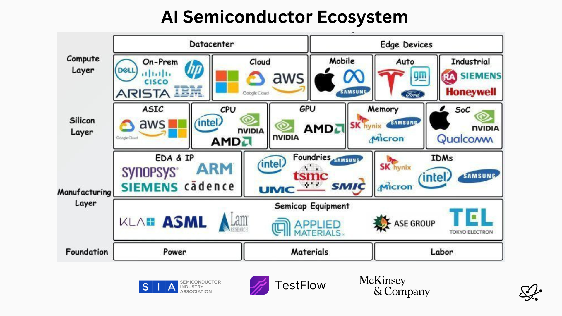
Executive Takeaways
- Hyperscale Disintermediation: The world’s largest cloud service providers—Google, Amazon, Microsoft, and Meta—are aggressively deploying proprietary ASICs (Application-Specific Integrated Circuits) to slash reliance on Nvidia, preserve enterprise operating margins, and optimize Total Cost of Ownership (TCO).
- The CUDA Defensive Trench: While competing silicon achieves raw floating-point parity on paper, Nvidia’s decade-plus software ecosystem moat (CUDA) and NVLink interconnect architectures continue to capture over 80% of data center training capital allocation.
- Packaging and Memory as True Chokepoints: The AI scaling race is no longer solely governed by nanometer lithography nodes; access to High Bandwidth Memory (HBM3e/HBM4) and advanced packaging capacity (specifically TSMC’s CoWoS) dictates real-world market supply.
- Inference vs. Training Divergence: A structural shift from monolithic foundation-model pre-training to distributed, low-latency token inference is creating unprecedented commercial openings for alternative architectures, including Linear Processing Units (LPUs) and analog in-memory compute engines.
The Compute Sovereign: Nvidia’s Dominance and the $1 Trillion Infrastructure Squeeze
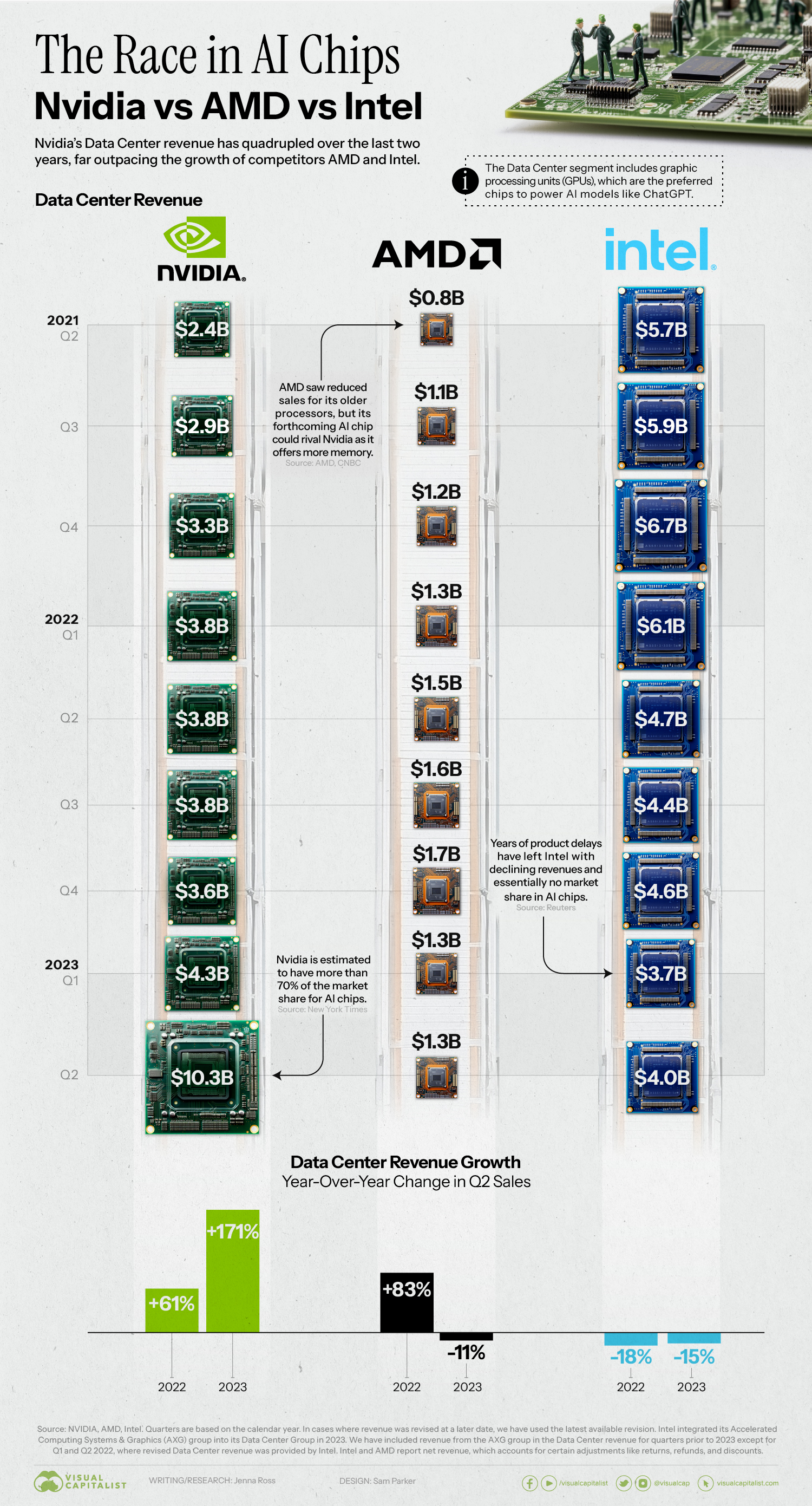
The global race for artificial general intelligence has transformed the semiconductor industry from a cyclical cyclical play into the geopolitical fulcrum of global enterprise finance. At the epicenter stands Nvidia Corp., whose market capitalization has defied historical valuation multiples on the back of its Hopper (H100/H200) and Blackwell (B200/GB200) architectures. Yet beneath the record-breaking quarterly data center revenues lies a complex institutional reality: enterprise clients are spending up to 85% of their AI infrastructure budgets solely on compute and interconnect hardware, triggering an unsustainable capital expenditure cycle that tech CFOs are desperate to rein in.
The structural vulnerability of this monoculture is financial as much as technical. Leading hyperscalers are projected to allocate more than $200 billion in aggregate capital expenditures over the next twelve months, with a staggering proportion funneling straight into Nvidia’s gross margins, which hover near 75%. To achieve viable enterprise ROI, mitigate single-supplier risk, and tailor silicon to idiosyncratic transformer workloads, a formidable coalition of merchant competitors, cloud titans, and venture-backed semiconductor upstarts has mobilized across the global compute stack.
Deconstructing the 30+ AI Chip Contenders
The challenger ecosystem can be systematically categorized into five distinct architectural echelons, each addressing specific performance vectors, latency thresholds, and power envelopes across the global enterprise workflow.
Tier 1: The Merchant Silicon Titans (Challengers to the Throne)
Nvidia’s traditional semiconductor peers are leveraging open software frameworks and aggressive interconnect standards to lure enterprise deployments away from the proprietary CUDA garden.
- Advanced Micro Devices (AMD): Armed with the Instinct MI300X and MI325X platforms, AMD represents the most proximate merchant threat. Utilizing a sophisticated multi-chiplet design pairing CDNA 3 architecture with 192GB of HBM3 memory, AMD targets memory-capacity-limited large language models (LLMs). AMD's primary enterprise lever is the open-source ROCm software stack, which has achieved functional maturity for mainstream frameworks like PyTorch and vLLM.
- Intel: Repositioning its data center roadmap, Intel’s Gaudi 2 and Gaudi 3 accelerators offer a cost-to-performance proposition aimed squarely at value-oriented enterprise inference and mid-scale training clusters. By integrating standard Ethernet interconnects directly onto the silicon substrate, Intel seeks to dismantle the prohibitive premium commanded by proprietary networking fabrics.
Tier 2: The Hyperscaler In-House ASICs (The Margin Protectors)
The most severe existential threat to Nvidia’s long-term top-line multiple does not stem from merchant competitors, but from its primary customers. The "Big Four" cloud providers are vertically integrating silicon design to internalize margins and optimize domain-specific models.
- Alphabet (Google TPU v5p & Trillium v6): The pioneer of hyperscale custom silicon, Google’s Tensor Processing Unit family powers everything from Gemini pre-training to external enterprise deployments within Google Cloud Platform, using custom optical circuit switches (OCS) for dynamic pod-level topology reconfigurations.
- Amazon Web Services (Trainium2 & Inferentia2): AWS is commoditizing enterprise AI training and deployment economics via proprietary silicon developed by its Annapurna Labs division, guaranteeing lower cost-per-inference metrics for AWS-native software ecosystems.
- Microsoft (Azure Maia 100): Engineered specifically for the Azure cloud architecture, Maia is optimized for OpenAI’s algorithmic demands, reducing Microsoft’s systemic reliance on Hopper allocations.
- Meta (MTIA v1 & v2): The Meta Training and Inference Accelerator focuses ruthlessly on ranking, recommendation systems, and ad-targeting inference, optimizing internal workloads that drive Meta’s core advertising revenue engine.
- Alibaba (Hanguang 800) & Baidu (Kunlunxin): Chinese cloud operators have aggressively advanced domestic ASIC development to safeguard cloud scalability against widening Western export restrictions.
Tier 3: The Next-Gen Structural & Disruptive Startups
Venture capital and sovereign wealth funds have flooded billions into clean-sheet architectural paradigms optimized for non-Von Neumann computing, token generation speed, and massive context windows.
- Groq: Pioneering the Language Processing Unit (LPU), Groq utilizes a deterministic Tensor Streaming Architecture that eliminates traditional HBM dependencies in favor of ultra-high-speed on-chip SRAM. This yields unmatched inference throughput (tokens per second) for auto-regressive language models.
- Cerebras Systems (Wafer-Scale Engine 3): Shattering conventional chipmaking limits, Cerebras crafts an entire silicon wafer into a single 4-trillion-transistor computing engine, bypassing the latency penalties inherent in packaging multiple discrete chips across a circuit board.
- Tenstorrent: Led by industry luminary Jim Keller, Tenstorrent champions modular, low-power RISC-V architectures and open-standard interconnect chiplets, creating a flexible compute paradigm that targets both cloud and edge workloads without proprietary IP lock-in.
- SambaNova Systems (SN40L): Employs a Reconfigurable Dataflow Architecture (RDA) that dynamically configures physical on-chip compute resources to mirror the underlying neural network graph, drastically reducing data movement.
- Etched: Focusing entirely on application-specific hard-wiring, Etched's "Sohu" ASIC burns the transformer attention mechanism directly into silicon, abandoning general programmability to deliver order-of-magnitude gains in inference throughput and energy efficiency.
- D-Matrix: Specializing in Digital In-Memory Computing (DIMC), D-Matrix eliminates memory-bandwidth bottlenecks for generative inference by executing calculations directly inside SRAM storage arrays.
- Untether AI & FuriosaAI: Developing spatial, at-memory compute architectures designed to optimize power-efficiency curves for vision-language models and enterprise real-time streaming services.
Tier 4: Edge AI, Automotive & Specialized Mobile Processing
As enterprise inference disperses outward from centralized hyper-scale server farms to client endpoints, laptops, smartphones, and autonomous vehicles, power constraints dictate silicon selection.
- Qualcomm (Cloud AI 100 & Snapdragon NPU): Dominating the client-side PC and smartphone tier, Qualcomm combines multi-core NPU processing to execute local generative AI models within tight 5W to 45W thermal envelopes.
- Apple (M-Series Neural Engine): Apple’s unified memory architecture allows consumer-grade silicon to retain high-parameter LLM weights locally in system memory, offering consumer and developer inference with unmatched energy efficiency.
- Hailo, Ambarella, & SiMa.ai: Dedicated vision and edge-intelligence silicon manufacturers delivering real-time sensory processing for industrial robotics, defense, and smart city infrastructure.
- Blaize, Axelera AI, & Kneron: Focused on cost-effective, decentralized edge inference, deploying proprietary neural network acceleration units to industrial IoT endpoints.
Tier 5: Sovereign Compute & Sanction-Resistant Architectures
Geopolitical bifurcation has fostered an independent domestic semiconductor ecosystem in East Asia, insulated from Western supply chains.
- Huawei (Ascend 910B & 910C): Built under profound technological constraints, the Ascend platform has emerged as the de facto sovereign infrastructure engine for the Chinese domestic ecosystem, backed by the CANN software architecture developed to mirror CUDA.
- Biren Technology, Moore Threads, & Enflame: Domestic Chinese GPU developers leveraging mixed architectural schemes to serve localized training and inference, navigating strict US Entity List lithography barriers.
Comparative Analysis: Archetypes of the AI Accelerator Landscape
The following audited table contrasts representative flagship architectures across critical enterprise metrics, highlighting hardware and commercial trade-offs.
| Provider & Processor | Architectural Classification | Primary Memory Architecture | Peak Theoretical Compute | Primary Moat / Enterprise Advantage | Primary Vulnerability / Headwind |
|---|---|---|---|---|---|
| Nvidia Blackwell B200 | General-Purpose Merchant GPU | 192GB HBM3e (8 TB/s) | 20 PFLOPS (FP4) / 9 PFLOPS (FP8) | Unrivaled CUDA ecosystem; NVLink 5 clustering scalability | High unit pricing; severe supply-chain allocation constraints |
| AMD Instinct MI300X | Merchant Compute Chiplet GPU | 192GB HBM3 (5.3 TB/s) | 2.6 PFLOPS (FP16/BF16) | Superior memory density per dollar; open-source ROCm stack | Lagging developer ecosystem adoption relative to CUDA |
| AWS Trainium2 | Custom Hyperscaler ASIC | Proprietary Shared HBM Fabric | Targeted at 4x Trainium1 throughput | Seamless AWS integration; hyper-optimized TCO for cloud tenants | Zero portability beyond AWS; strictly single-platform ecosystem |
| Groq LPU | Deterministic Tensor Streaming (LPU) | 230MB On-Chip SRAM (80 TB/s) | 750 TFLOPS (FP16) | Sub-millisecond inference latency; massive tokens/sec output | Extremely low memory capacity per chip; requires massive clustering |
| Cerebras WSE-3 | Monolithic Wafer-Scale Engine | 44GB On-Chip SRAM (21 PB/s) | 125 PFLOPS (FP16) | Zero off-die clustering latency; massive parallel compute density | Bespoke liquid-cooling and power-distribution infrastructure required |
| Huawei Ascend 910B | Sovereign Enterprise NPU | 32GB/64GB HBM2e | Equivalent to legacy A100 tiers | Guaranteed domestic market capture; state-backed procurement | Sanctioned foundry access; packaging yield limitations |
Industry & Market Implications: The TCO Paradigm Shift
The ongoing silicon diversification represents an essential phase change in enterprise capital allocation. For the past three years, the corporate playbook dictated stockpiling general-purpose GPUs to hedge against hardware scarcity. However, as the initial generative AI wave transitions from model exploration to industrial production, CFOs are demanding that engineering leaders optimize for **inference economics** rather than raw training muscle.
Inference workloads present fundamentally different architectural demands than training. While training requires colossal memory scale and precision floating-point arithmetic to calculate backpropagation gradients, inference is heavily bottlenecked by memory bandwidth and latency—retrieving model weights sequentially to output individual tokens. This operational divergence is where specialized ASICs, LPUs, and in-memory compute engines present a compelling enterprise ROI calculus: they run production models at fractions of the hardware acquisition cost and power consumption necessitated by full-scale GPU clusters.
Concurrently, the manufacturing bottleneck remains an inescapable geopolitical vulnerability. Nearly every merchant and hyperscale architecture—with the exception of sanctioned domestic alternatives—relies entirely on Taiwan Semiconductor Manufacturing Company (TSMC) for both front-end sub-5nm lithography and back-end Chip-on-Wafer-on-Substrate (CoWoS) advanced packaging. Consequently, while the market may fragment across dozens of chip *designers*, the operational risk of the global AI economy remains concentrated along a narrow geographical axis.
Frequently Asked Questions (People Also Ask)
Can any competitor realistically break Nvidia’s CUDA software ecosystem moat?
Nvidia’s software ecosystem, CUDA (Compute Unified Device Architecture), has been actively developed and integrated into academic and enterprise computer-science workflows since 2006. Dislodging it is extraordinarily difficult because millions of lines of proprietary enterprise code, libraries, and runtime orchestrations are hard-coded to CUDA primitives. However, cross-platform abstraction frameworks such as OpenAI’s Triton, PyTorch 2.0, and Google’s OpenXLA compiler are abstracting the hardware layer away from underlying architectures. This allows engineers to compile neural networks onto AMD (ROCm), Intel, or custom ASICs with minimal code modification, steadily eroding CUDA's defensive moat over time.
What is the fundamental difference between GPUs, ASICs, and LPUs for AI?
A Graphic Processing Unit (GPU) is a highly parallel, yet generally programmable processor capable of executing diverse mathematical workloads, making it ideal for experimental AI model development and training. An Application-Specific Integrated Circuit (ASIC)—such as Google's TPU or AWS's Inferentia—is custom-tailored at the hardware level for specific mathematical calculations (like matrix multiplications), sacrificing general programmability in exchange for vastly superior energy efficiency, lower cost, and high throughput. A Language Processing Unit (LPU), like that designed by Groq, uses deterministic architectures relying on hyper-fast on-chip SRAM to streamline inference, processing sequential token generation significantly faster than memory-bound GPUs.
Why are cloud hyperscalers spending billions to design their own silicon?
The economic logic for hyperscalers (Amazon, Microsoft, Google, Meta) is rooted in margin preservation and platform stickiness. Relying exclusively on Nvidia forces hyperscalers to accept structural gross margin compression, as hardware profits are retained by Nvidia rather than the cloud operator. By deploying in-house silicon, cloud providers reduce the cost of running internal consumer services (e.g., search, dynamic ad-targeting, video ranking), while concurrently offering enterprise cloud clients lower-cost compute options, thereby establishing sustainable competitive pricing advantages.
What is the primary constraint limiting the production volume of AI chips?
The primary manufacturing throttle is not the production of standard silicon wafers, but rather advanced 2.5D and 3D packaging technologies—specifically TSMC's CoWoS (Chip-on-Wafer-on-Substrate)—alongside the finite global supply of High Bandwidth Memory (HBM3e and HBM4). Advanced AI chips require heterogeneous integration, placing logic dies directly adjacent to multiple HBM stacks on a microscopic silicon interposer. The extreme precision and thermal complexity involved in this process create structural supply ceilings that even the best-capitalized semiconductor giants cannot quickly bypass.
Future Outlook: The Road to 2026 and Beyond
The hyper-accelerated AI hardware ecosystem is rapidly approaching several transformative milestones that will reshape enterprise compute valuation multiples through the end of the decade:
- The HBM4 Architectural Leap: The debut of next-generation HBM4 memory stacks will transition the base logic die from standard DRAM manufacturing to custom foundry logic processes (such as 3nm and 4nm nodes), enabling unprecedented memory bandwidth and tighter integration directly with the compute host.
- Silicon Photonics Integration: As copper-based interconnects reach fundamental physical and thermal limits across enterprise server racks, optical I/O and co-packaged optics (CPO) will become mandatory to sustain inter-chip communications at multi-terabit bandwidth thresholds.
- Inference Dominating Enterprise Budgets: The capital expenditure mix between AI training and AI inference is projected to shift from parity to a dramatic 20/80 divergence by 2027. This shift will structurally benefit lower-cost, domain-specific ASIC architectures, while forcing Nvidia to aggressively iterate its software abstractions and networking hardware to maintain its premier enterprise margins.