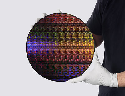
IBM Shatters Silicon Limits: Debuts World’s First Sub-1 Nanometer Chip to Power the Next AI Supercycle
The historic breakthrough utilizes a revolutionary "nanostack" 3D architecture, packing 100 billion transistors into a fingernail-sized footprint to salvage AI’s compounding energy crisis.
NEW YORK & BENGALURU — In a monumental leap that effectively rewrites the roadmap of global semiconductor physics, IBM has officially debuted the world’s first sub-1 nanometer (nm) chip technology. The announcement, dispatched from IBM’s flagship research facility, marks the first time humanity has engineered silicon-based logic elements at a sub-atomic scale, specifically utilizing a physical channel width equivalent to just 15 rows of silicon (Si) atoms.
By leveraging an entirely new, proprietary "nanostack" 3D chip architecture, IBM’s prototype successfully packs nearly 100 billion transistors onto a slice of silicon no larger than a human fingernail. The breakthrough arrives at a critical juncture for the global technology sector, where the exponential power demands of generative artificial intelligence are pushing existing 3nm and 2nm infrastructure to the brink of power grid exhaustion.
Inside the 'Nanostack' Breakthrough: How IBM Defied Physics

For the past decade, semiconductor physicists have warned of the imminent death of Moore’s Law—the observation that the number of transistors on a microchip doubles roughly every two years. At sub-2nm levels, traditional horizontal nanosheet designs suffer from severe "quantum tunneling," a phenomenon where electrons slip through physical barriers, causing catastrophic current leakage and overheating.
IBM’s Albany, New York-based research division bypassed this structural dead-end through its radical "nanostack" 3D architecture. Instead of placing nanosheets side-by-side, the sub-1nm technology vertically stacks active transistor channels. By refining the lithography down to a scale of just 15 silicon atoms wide, IBM has engineered a gate-all-around (GAA) structure that provides unprecedented electrostatic control over the flow of electrons.
According to preliminary benchmark data released by the IBM Newsroom, this architecture delivers a staggering 45% performance increase or a 75% reduction in energy consumption compared to today's state-of-the-art 3nm commercial chips.
Key Executive Takeaways
- The Density Frontier: Fits approximately 100 billion transistors into a fingernail-sized die, doubling the density of projected 2nm commercial nodes.
- The 15-Atom Channel: Reaches the absolute physical limit of silicon-based material science, utilizing a channel width of just 15 silicon atoms.
- AI Optimization: Specifically architected to accelerate matrix multiplication on-chip, drastically lowering the power required to train and run Large Language Models (LLMs).
- Geopolitical Shift: Reasserts Western intellectual property dominance in the upstream semiconductor design pipeline, altering the leverage dynamics between the US, East Asia, and European manufacturing hubs.
The Geopolitical and Market Impact: TSMC, Samsung, and Intel on Notice
IBM’s announcement has sent shockwaves through the global technology supply chain, catching competitors and foundry giants off guard. While IBM transitioned to a fabless model years ago—focusing on IP creation rather than high-volume manufacturing—it licenses its foundational breakthroughs to major fabrication players, including Samsung and Intel.
Industry analysts suggest that this sub-1nm breakthrough will dramatically intensify the race between Taiwan Semiconductor Manufacturing Co. (TSMC), Samsung Electronics, and Intel's Foundry Services. Currently, TSMC and Samsung are racing to commercialize 2nm nodes by late 2025 or early 2026. IBM’s leap directly to sub-1nm completely bypasses the projected timelines of the major foundries, offering a blueprint for the next decade of hardware manufacturing.
"This isn't an incremental step; it is a fundamental reimagining of silicon chemistry," said an industry-leading hardware analyst. "With the energy grids of the US, Europe, and India buckling under the weight of massive AI data centers, a chip that cuts power consumption by three-quarters while maintaining computing throughput is the holy grail of modern tech infrastructure."
Comparative Technology Roadmap
To understand the scale of IBM’s achievement, it is necessary to compare the new sub-1nm node against current industry standards and near-term projections:
| Chip Node Era | Primary Architecture | Est. Transistor Density (per mm²) | Primary Limitation / Advantage |
|---|---|---|---|
| 3nm (Current State) | Nanosheet / FinFET | ~200–290 Million | High thermal leakage at peak AI processing loads. |
| 2nm (Projected 2025/26) | Horizontal Nanosheet (GAA) | ~310–330 Million | Nearing the physical limits of horizontal scaling. |
| Sub-1nm (IBM Breakthrough) | "Nanostack" 3D GAA (15 Si Atoms) | Over 600 Million | Virtually eliminates quantum tunneling; 75% power reduction. |
The Road to Commercialization: Overcoming the EUV Hurdle
While the hardware community is celebrating the breakthrough, industrial-scale deployment remains a multi-year engineering challenge. Manufacturing a sub-1nm chip requires highly specialized High-NA (High Numerical Aperture) Extreme Ultraviolet (EUV) lithography systems, which are currently produced exclusively by the Dutch conglomerate ASML.
IBM must now work alongside its ecosystem partners to transition the "nanostack" process from the controlled, sterile environment of its Albany Research Lab to commercial high-volume foundries. Industry insiders predict that while the technology will first integrate into specialized cloud supercomputers and national defense defense systems by late 2028, it may not reach consumer smartphones and mainstream AI servers until approximately 2030.
Nevertheless, by demonstrating the absolute viability of silicon at the sub-1nm threshold, IBM has successfully cleared a path forward for the global digital economy, ensuring that the relentless drive toward artificial general intelligence (AGI) will not be starved of the computational power it desperately requires.
Frequently Asked Questions
What is "nanostack" 3D architecture, and how does it differ from traditional chip design?
Traditional chips place transistors horizontally across a flat plane. As transistors shrink, they run out of physical space, causing electrical leakage. IBM's "nanostack" 3D architecture solves this by stacking the active nanosheet channels vertically. This 3D scaling allows nearly 100 billion transistors to sit on a fingernail-sized chip while maintaining precise electrical control, dramatically reducing power consumption.
When will consumers see sub-1nm chips in everyday devices?
While IBM has successfully proven and debuted the sub-1nm technology in a lab environment, commercial production is a complex process. Foundries must first integrate IBM’s patents into their High-NA EUV lithography lines. Industry experts project that the first sub-1nm chips will debut in enterprise AI data centers and defense systems by 2028, with broader consumer electronics adoption expected around 2030.