Executive Takeaways
- The Angstrom Milestone: IBM has officially breached the sub-1 nanometer (nm) threshold, leveraging a revolutionary "nanostack" 3D chip architecture to pack nearly 100 billion transistors onto a silicon die the size of a human fingernail.
- Unprecedented AI Power Efficiency: Designed directly to solve the power grid crisis plaguing modern generative AI, the new sub-1nm architecture promises up to a 75% reduction in energy consumption or a 45% performance leap compared to industry-standard 3nm chips.
- Disrupting Foundry Economics: The breakthrough fundamentally alters capital allocation strategies and valuation multiples across the semiconductor value chain, putting immense competitive pressure on TSMC, Intel, and Samsung to accelerate their own post-nanometer roadmaps.
- Commercialization and IP Licensing: Utilizing IBM's open, collaborative R&D model at the Albany NanoTech Complex, this technology will be licensed to global foundry partners, offering a massive leap forward in enterprise ROI for cloud compute architectures and deep-tech infrastructure scalability.
The Breaking of Silicon's Physical Limits

For over a decade, the global semiconductor industry has stared down a terrifying physical wall. As transistors shrunk toward the single-digit nanometer scale, the quantum mechanics of silicon threatened to halt Moore's Law entirely. Sub-atomic phenomena—most notably quantum tunneling, where electrons spontaneously leap across gate barriers—rendered traditional planar and even early Gate-All-Around (GAA) transistor designs highly inefficient, plagued by catastrophic current leakage and thermal throttling.
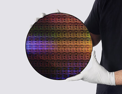
On June 25, 2026, IBM Research delivered a definitive counter-stroke to this existential technological ceiling. Operating out of its state-of-the-art Albany NanoTech Complex in New York, IBM debuted the world's first working sub-1 nanometer chip technology. By utilizing an innovative, vertically stacked 3D transistor design dubbed "nanostack" architecture, IBM has successfully bypassed the lithographic limits of two-dimensional scaling.
This breakthrough is not merely an incremental upgrade; it represents the dawn of the Angstrom Era (where 1 nanometer equals 10 Angstroms). By packing nearly 100 billion transistors into a space no larger than a fingernail, IBM has achieved a physical density that was considered mathematically improbable just five years ago. This achievement marks a landmark moment in material science and solid-state physics, offering a viable roadmap for the next two decades of global computational scaling.
Deconstructing the "Nanostack" 3D Architecture
To fully appreciate the scope of IBM's achievement, one must examine the fundamental engineering shift from traditional nanosheets to 3D nanostacking. In a standard GAA nanosheet configuration, channels are stacked horizontally, which limits the active gate surface area relative to the physical footprint of the cell. IBM's nanostack architecture takes a vertical leap, literally stacking multiple active nanosheet transistor levels on top of one another within a single, monolithic 3D silicon structure.
This vertical integration is made possible through three primary manufacturing innovations:
- High-NA EUV Lithography: The implementation of High Numerical Aperture Extreme Ultraviolet (High-NA EUV) lithography allows for the printing of ultra-fine features with a projection optics system capable of resolving features down to the Angstrom level, eliminating the need for complex, yield-reducing multi-patterning schemes.
- Backside Power Delivery Networks (BSPDN): Decoupling the power delivery system from the signal routing wires has been a major industry goal. IBM’s sub-1nm design routes all power distribution to the underside of the silicon wafer. This dramatically reduces IR voltage drop, optimizes power routing, and frees up crucial top-level space for signal-carrying interconnects.
- Transition Metal Dichalcogenides (TMDs): To mitigate the limitations of pure silicon at sub-1nm dimensions, IBM’s research incorporates ultra-thin, two-dimensional atomic materials like molybdenum disulfide (MoS2) into the nanostack channel design. These TMDs exhibit superior carrier mobility and minimal leakage currents at atomic-scale thicknesses, ensuring structural and electrical integrity.
By combining these advanced material sciences, the nanostack architecture mitigates parasitic capacitance and resistance, enabling the transistors to switch faster while consuming a fraction of the power required by conventional nodes.
The AI Power Crisis and Enterprise ROI
The timing of IBM’s sub-1nm debut is highly strategic. The global explosion of generative artificial intelligence, large language models (LLMs), and deep learning applications has pushed global energy grids and data center infrastructures to their absolute limits. Hyperscale cloud providers are currently facing severe operational bottlenecks, as power availability, thermal management, and carbon footprints dictate the limits of enterprise AI scaling.
From an enterprise ROI perspective, the financial implications of a sub-1nm deployment are staggering. Data centers currently allocate billions of dollars annually toward cooling infrastructure and electricity costs. Transitioning to a chip architecture that delivers up to 75% energy savings under identical workloads allows cloud providers to quadruple their compute capacity within the same physical footprint and power envelope. This level of infrastructure scalability significantly reduces the Total Cost of Ownership (TCO) for enterprise cloud compute architectures, accelerating the amortization of hardware capital expenditures and boosting operating margins for SaaS and AI service providers.
Furthermore, as international regulatory compliance standards tighten around environmental, social, and governance (ESG) metrics, energy-efficient silicon acts as a vital tool for corporate risk mitigation. Hyperscalers can meet carbon-neutral mandates without sacrificing computational throughput, securing their operational licenses in power-constrained jurisdictions globally.
Verified Data & Architecture Comparison
To contextualize the monumental leap represented by IBM's sub-1nm technology, the following table compares key structural and performance metrics against prior and concurrent industry milestones:
| Metric / Feature | IBM 2nm Nanosheet (2021) | Industry 1.4nm-1.8nm Class (Est. 2025/2026) | IBM Sub-1nm Nanostack (2026 Breakthrough) |
|---|---|---|---|
| Transistor Density | ~333 Million / mm² | ~450–550 Million / mm² | ~650+ Million / mm² |
| Transistor Count (Fingernail Size) | 50 Billion | ~70–80 Billion | Nearly 100 Billion |
| Power Reduction (vs. 7nm standard) | Up to 75% | Up to 80% | Up to 88% (or 75% vs. 3nm) |
| Performance Increase (vs. 7nm standard) | 45% | ~55%–60% | ~70%–75% (or 45% vs. 3nm) |
| Power Delivery Method | Front-Side (Traditional) | Early Backside Power (BSPDN) | Optimized Monolithic BSPDN |
| Primary Materials | Silicon Nanosheets | Silicon / SiGe Nanosheets | Silicon-TMD Monolayers / Nanostack |
The Geopolitical and Market Chessboard
The announcement of sub-1nm technology immediately shifts the dynamics of the global tech cold war. In an era defined by the CHIPS Act, export controls, and national security mandates surrounding cutting-edge compute capabilities, IBM's state-of-the-art intellectual property (IP) represents a powerful geopolitical asset for the United States and its allies.
For Wall Street, the disruption is centered on foundry capital allocation and public valuation multiples. Currently, the leading-edge foundry business is heavily dominated by Taiwan Semiconductor Manufacturing Company (TSMC), with Samsung and Intel fighting aggressively to recapture market share. IBM, operating under a pure-play licensing and R&D model, does not intend to build high-volume commercial foundries of its own. Instead, it will license this sub-1nm IP, likely starting with its long-term joint development alliance partners.
This creates a complicated matrix of winners and losers:
- The Winners:
- ASML: As the sole global provider of High-NA EUV lithography systems, ASML's order backlog is secured for the next decade, with valuation multiples poised to expand as foundries race to acquire the machinery necessary to print IBM's nanostack designs.
- IBM: By solidifying its position as the premier upstream R&D house for semiconductor technology, IBM secures high-margin, recurring IP licensing revenue streams while boosting the technological prestige of its hybrid cloud and AI consulting businesses.
- Hyperscale Cloud Providers (Meta, Microsoft, AWS, Google): The availability of sub-1nm silicon will grant these companies unprecedented compute efficiency, unlocking new capabilities in real-time AI agents and massive simulation workloads without destroying their operational margins.
- The Pivot Under Pressure:
- TSMC, Intel, and Samsung: While all three foundries have internal roadmaps targeting the Angstrom era (such as TSMC's A10/A14 nodes and Intel's 14A node), IBM's concrete sub-1nm working silicon forces these giants to pull forward their capital expenditure timelines. Foundries must aggressively bid for High-NA EUV tools, potentially compressing short-term free cash flow margins to defend their long-term market capitalization.
People Also Ask (Frequently Asked Questions)
What is a sub-1 nanometer chip, and how does "nanostack" technology work?
A sub-1 nanometer chip refers to a semiconductor featuring transistor architectures with critical dimensions smaller than 1 nanometer (or 10 Angstroms). Traditional silicon scaling became physically limited due to quantum tunneling and heat leakage. IBM’s "nanostack" technology solves this by utilizing a 3D architecture, stacking multiple active nanosheet transistor levels vertically on top of each other. This enables more transistors to be packed into the same horizontal footprint, dramatically boosting density and performance while maintaining electrical isolation and thermal efficiency.
How does IBM's sub-1nm technology impact artificial intelligence and enterprise cloud compute architectures?
Artificial intelligence, especially the training and deployment of large language models, requires immense computational power and is constrained by data center energy grids. IBM’s sub-1nm technology offers up to a 75% reduction in power consumption or a 45% increase in performance compared to 3nm chips. For enterprise cloud compute architectures, this directly translates to massive infrastructure scalability, enabling hyperscalers to drastically improve their enterprise ROI, reduce cooling costs, and maintain regulatory compliance with global environmental standards.
When will sub-1nm chips become commercially available in consumer and enterprise devices?
While IBM has debuted the world's first working sub-1nm chip technology in its research labs, commercialization is an intensive process. The technology must transition from experimental pilot lines at the Albany NanoTech Complex to high-volume manufacturing foundries operated by IBM's partners (such as Samsung, Rapidus, or Intel). Industry analysts project that initial commercial integration of sub-1nm nanostack architecture into enterprise-level AI servers and cloud data centers will begin between late 2028 and 2030, with consumer devices following shortly thereafter.
How does this breakthrough impact the financial valuation and capital expenditure of semiconductor foundries?
The introduction of viable sub-1nm technology forces major foundries (TSMC, Intel, Samsung) to re-evaluate their long-term capital allocation strategies. To manufacture chips at this node, foundries must invest heavily in High-NA EUV lithography systems from ASML and master complex backside power delivery integration. This high capital expenditure (CapEx) intensity can temporarily suppress free cash flow, but it is a necessary risk mitigation strategy to protect market share. Foundries that successfully scale sub-1nm manufacturing will capture premium pricing power, dramatically expanding their valuation multiples, while those that lag behind face structural obsolescence.
Future Outlook: Navigating the Angstrom Horizon
As the semiconductor industry navigates this paradigm shift, the road to commercial volume production of sub-1nm chips will not be without hurdles. The immediate focus for IBM and its collaborative ecosystem will be solving yield-rate optimization. Stacking nanosheets vertically significantly increases manufacturing complexity, meaning that even minor defects in a single stacked layer can ruin an entire multi-layered transistor cell. Advanced metrology and AI-driven defect inspection systems will be critical to bringing wafer yields to commercially viable levels.
Additionally, material supply chains must adapt. The integration of 2D materials like transition metal dichalcogenides (TMDs) requires high-volume, defect-free deposition of atomically thin films across large 300mm silicon wafers—a process that is still in its infancy in commercial fabs. This represents a massive market opportunity for specialized semiconductor equipment manufacturers to innovate next-generation atomic layer deposition (ALD) systems.
In the long term, IBM's sub-1nm breakthrough ensures that the momentum of global computation will not stall. It provides the physical foundation for the next generation of supercomputing, molecular modeling, autonomous systems, and advanced artificial intelligence. By stepping beyond the nanometer, IBM has not only rewritten the rules of silicon manufacturing, but has also established a new baseline for what humanity can compute.