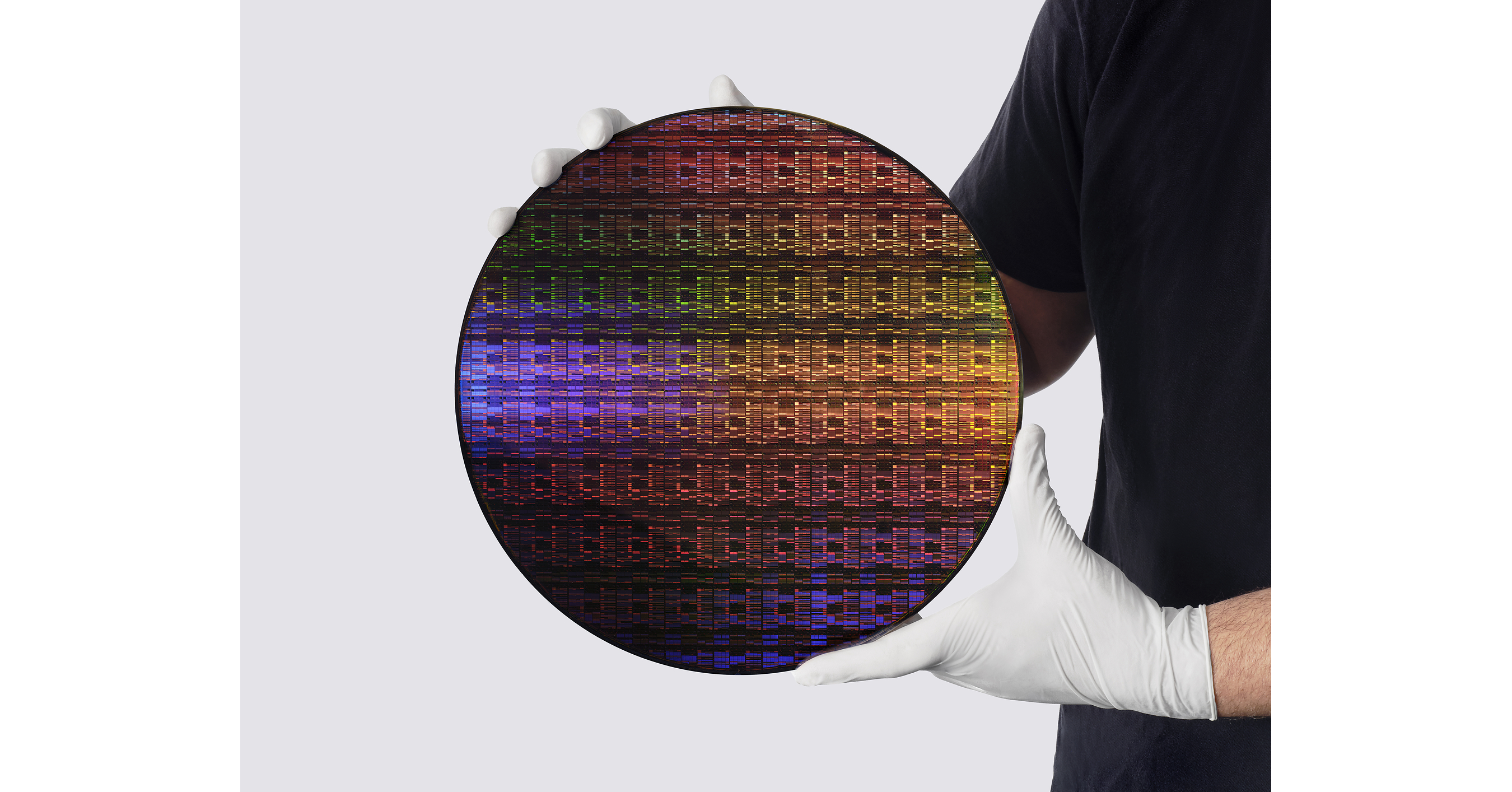
NEW YORK — In a monumental leap for global semiconductor engineering, IBM has officially pulled back the curtain on the world’s first sub-1 nanometer chip technology. Announced today via the IBM Newsroom, the breakthrough effectively rewrites the roadmap for computing power, artificial intelligence infrastructure, and consumer electronics for the next decade.
The landmark development shatters long-standing industry doubts regarding the physical limitations of silicon scaling. By defying conventional scaling boundaries, IBM’s new architecture promises to pack nearly 100 billion transistors onto a single piece of silicon no larger than a human fingernail, unlocking unprecedented computational density and energy efficiency.
The Engineering Marvel: Inside the 'Nanostack' 3D Architecture
At the heart of IBM’s breakthrough is a proprietary, revolutionary design known as "nanostack" 3D chip architecture. Unlike traditional planar designs or early 3D vertical stacking methods that suffer from severe thermal bottlenecks and signal interference, the nanostack configuration allows transistors to be woven vertically with atomic precision.
Industry analysts note that moving into the sub-1 nanometer regime—historically considered a thermodynamic and quantum-tunneling wall for traditional semiconductor manufacturing—requires entirely new physics models. IBM’s research teams circumvented these hurdles by introducing novel gate-all-around (GAA) material variants and electrostatic shielding layers.
- Unprecedented Density: Packs nearly 100 billion transistors onto a fingernail-sized die.
- Thermal Efficiency: Utilizes advanced nanostack heat-dissipation pathways to prevent localized thermal throttling.
- Power Reductions: Expected to deliver up to 50% lower power consumption compared to current 2nm commercial nodes.
- AI Acceleration: Native hardware architecture optimized for massive Large Language Model (LLM) training and edge inference.
Market Impact and Economic Ripple Effects

The announcement sends immediate shockwaves through the global technology, finance, and geopolitical sectors. As generative AI models scale exponentially, data centers face crippling power constraints and hardware bottlenecks. IBM’s sub-1 nm breakthrough offers an immediate blueprint for sustainable hyperscale computing.
Wall Street analysts have reacted swiftly, projecting a massive realignment in capital expenditure among major cloud providers—including Amazon Web Services, Microsoft Azure, and Google Cloud—as they race to secure next-generation silicon partnerships. Furthermore, the technology is expected to radically transform edge computing, allowing smartphones, autonomous vehicles, and medical devices to run enterprise-grade artificial intelligence locally without relying heavily on remote cloud clusters.
| Metric / Feature | Previous Generation (2nm Class) | IBM Sub-1 Nanometer Technology |
|---|---|---|
| Transistor Count | ~50 billion per die | Nearly 100 billion per die |
| Architecture Style | Standard FinFET / Early GAA | Revolutionary "Nanostack" 3D Architecture |
| Energy Efficiency | Baseline | Up to 50% reduction in power draw |
| Primary Target | General computing & early AI | Hyperscale AI, LLMs, & Edge computing |
Looking Ahead: The Commercialization Timeline
While today’s unveiling marks a historic scientific milestone, industry experts emphasize that mass commercial fabrication will require significant tooling upgrades across global foundries. IBM plans to license its nanostack technology to key manufacturing partners, with pilot-line enterprise testing slated to begin late next year, and broader commercial availability expected toward the end of the decade.
As the global semiconductor race enters uncharted territory, IBM’s sub-1 nanometer achievement proves that rumors of the death of Moore’s Law have been greatly exaggerated. Instead, the industry is entering a new, hyper-dense era of three-dimensional computing.
Frequently Asked Questions
What is a sub-1 nanometer chip, and why is it important?
A sub-1 nanometer chip features transistors and gate structures measuring less than 1 nanometer in scale. This scale allows manufacturers to pack exponentially more computing power into tighter spaces, drastically increasing processing speeds while reducing electrical resistance and power consumption.
When will consumers be able to buy devices powered by IBM’s sub-1 nm technology?
IBM is currently showcasing the technology for enterprise and research validation. Commercial integration into enterprise data centers, AI accelerators, and high-performance consumer hardware is projected to roll out progressively over the next three to five years as manufacturing partners adapt fabrication lines to the nanostack architecture.