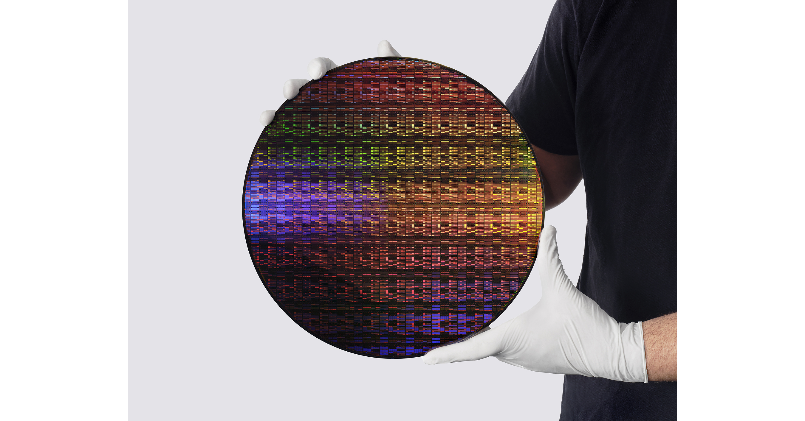
NEW YORK & BENGALURU — In a move that redrafts the geopolitical and technological roadmap of the global semiconductor industry, IBM has announced the debut of the world’s first sub-1 nanometer (nm) silicon chip technology. The breakthrough, announced early Thursday via the IBM Newsroom, represents a landmark achievement in materials science and processor architecture, potentially securing a massive leap forward in processing power just as the global artificial intelligence boom threatens to outstrip the world's energy grids.
Built using a revolutionary, proprietary "nanostack" 3D chip architecture, IBM’s sub-1nm technology successfully packs an astonishing 100 billion transistors onto a slice of silicon no larger than a human fingernail. The milestone effectively bypasses what many physicists believed was the absolute physical limit of silicon-based scaling, promising to unlock unprecedented computational efficiencies and massive power savings for next-generation AI workloads.
Executive Summary: The Sub-1nm Breakthrough at a Glance
- The Threshold Crossed: IBM becomes the first entity globally to design and demonstrate operational semiconductor architecture below the 1-nanometer threshold.
- The "Nanostack" Innovation: Shifting away from traditional horizontal and early-stage vertical nanosheet designs, IBM’s 3D "nanostack" allows multiple active transistor layers to be built vertically, maximizing density without increasing the chip's physical footprint.
- Unprecedented Density: Nearly 100 billion transistors are integrated onto a single fingernail-sized die, yielding a massive leap in processing speed.
- The Green AI Imperative: The architecture is projected to deliver up to a 75% reduction in energy consumption compared to today's leading-edge 3nm commercial chips, addressing the tech sector's pressing carbon footprint crisis.
Inside the "Nanostack" 3D Architecture: How IBM Defied Physics

For the past decade, chip designers have been warning of the imminent demise of Moore’s Law—the observation that the number of transistors on a microchip doubles roughly every two years. As transistors shrunk toward the 2nm and 1nm barriers, quantum tunneling (where electrons leap across barriers unpredictably) threatened to render traditional silicon switches useless.
IBM’s Zurich and Albany research teams overcame this barrier by rethinking transistor geometry entirely. The sub-1nm architecture utilizes a novel "nanostack" 3D structure. Instead of placing transistors side-by-side or in simple vertical nanosheets, IBM has stacked multiple atomic-thin channels on top of one another within a single 3D block, utilizing advanced gate-all-around (GAA) controls and custom-engineered insulating materials to prevent electrical leakage.
"This is not just an incremental step; it is a fundamental shift in how we build computers," said a senior IBM Fellow associated with the Albany NanoTech Complex. "By moving into a true three-dimensional nanostack, we have created a pipeline where electrons can be guided with near-zero resistance, achieving densities that were deemed mathematically impossible a few years ago."
The Silicon Comparison: How Sub-1nm Compares to Current Standards
To understand the scale of IBM’s achievement, it is helpful to compare the new sub-1nm technology against the current state-of-the-art commercial and experimental nodes currently in development by global foundries:
| Metric / Feature | Current Industry Standard (3nm) | Upcoming Next-Gen (2nm) | IBM Sub-1nm "Nanostack" |
|---|---|---|---|
| Transistor Count (Fingernail Size) | ~15 to 20 Billion | ~50 Billion (Projected) | ~100 Billion |
| Primary Architecture | FinFET / Early Nanosheet | Nanosheet (GAA) | 3D "Nanostack" GAA |
| Power Efficiency Gain | Baseline | ~45% improvement vs 3nm | ~75% improvement vs 3nm |
| Primary Applications | Consumer Electronics, Mobile | High-Performance Computing | Generative AI, Quantum-Bridge, Hyperscale Data Centers |
The Geopolitical and AI Energy Imperative
The timing of IBM’s breakthrough is highly strategic. Hyperscale data centers run by giants like Microsoft, Google, AWS, and Meta are currently consuming vast amounts of electricity to train and run massive Large Language Models (LLMs). Analysts estimate that by 2030, AI data centers could consume up to 10% of the United States' total grid output if efficiency does not improve.
By offering a 75% power reduction at equivalent performance levels, IBM’s sub-1nm technology could allow tech conglomerates to quadruple their AI processing capacity without expanding their energy footprints. This has massive cost-saving implications for cloud infrastructure providers who are currently bottlenecked by power grid constraints.
Furthermore, this development shifts the balance of power in the global chip race. While manufacturing giants like TSMC, Samsung, and Intel have been racing to commercialize their own 2nm and 1.4nm nodes by late 2027, IBM’s research-level leap to sub-1nm secures a vital intellectual property moat for Western chip design, heavily influencing future technology licensing and joint-venture manufacturing agreements.
The Road to Commercialization: When Will It Hit the Market?
As with all fundamental semiconductor breakthroughs, the transition from IBM's state-of-the-art laboratory at the Albany NanoTech Complex to high-volume commercial fabrication plants (fabs) will take time. IBM operates on a licensing and partnership model, meaning it will work alongside manufacturing partners like Samsung and potentially Intel to scale this technology for commercial deployment.
Industry analysts expect the first test runs of sub-1nm commercial chips to begin appearing in specialized foundries by late 2029, with widespread deployment in enterprise AI systems and defense supercomputers slated for the early 2030s.
Frequently Asked Questions (FAQ)
1. Does this mean Moore’s Law is officially alive?
Yes, but with a major catch. Classical physical scaling—where transistors were simply shrunk horizontally on a flat plane—is indeed dead. IBM’s breakthrough proves that Moore's Law will survive through vertical dimensional scaling (3D "nanostacking") and novel molecular materials rather than traditional horizontal lithography alone.
2. How does the sub-1nm technology solve the problem of power grid overload from AI?
Because the 3D nanostack architecture positions transistors closer together with atomic precision, signals travel shorter distances with far less electrical resistance. This allows processors to perform the trillions of calculations required by neural networks using only a fraction of the voltage required by current 3nm and 5nm processors, translating to an estimated 75% drop in overall energy consumption.