Executive Takeaways
- The Sub-1nm Breakthrough: IBM has officially unveiled the world’s first sub-1 nanometer semiconductor technology, operating at an astonishing 0.7-nanometer node.
- Revolutionary Architecture: Moving past traditional planar and standard FinFET paradigms, the new chips utilize a proprietary "nanostack" 3D architecture designed to bypass quantum leakage constraints.
- AI Compute Economics: The design targets exponential efficiency gains, offering dramatic power savings crucial for scaling enterprise AI inference and hyper-scale cloud data centers.
- Capital Expenditure Shifts: The milestone fundamentally alters valuation multiples, semiconductor supply chain capital allocation, and long-term risk mitigation strategies for global foundries.
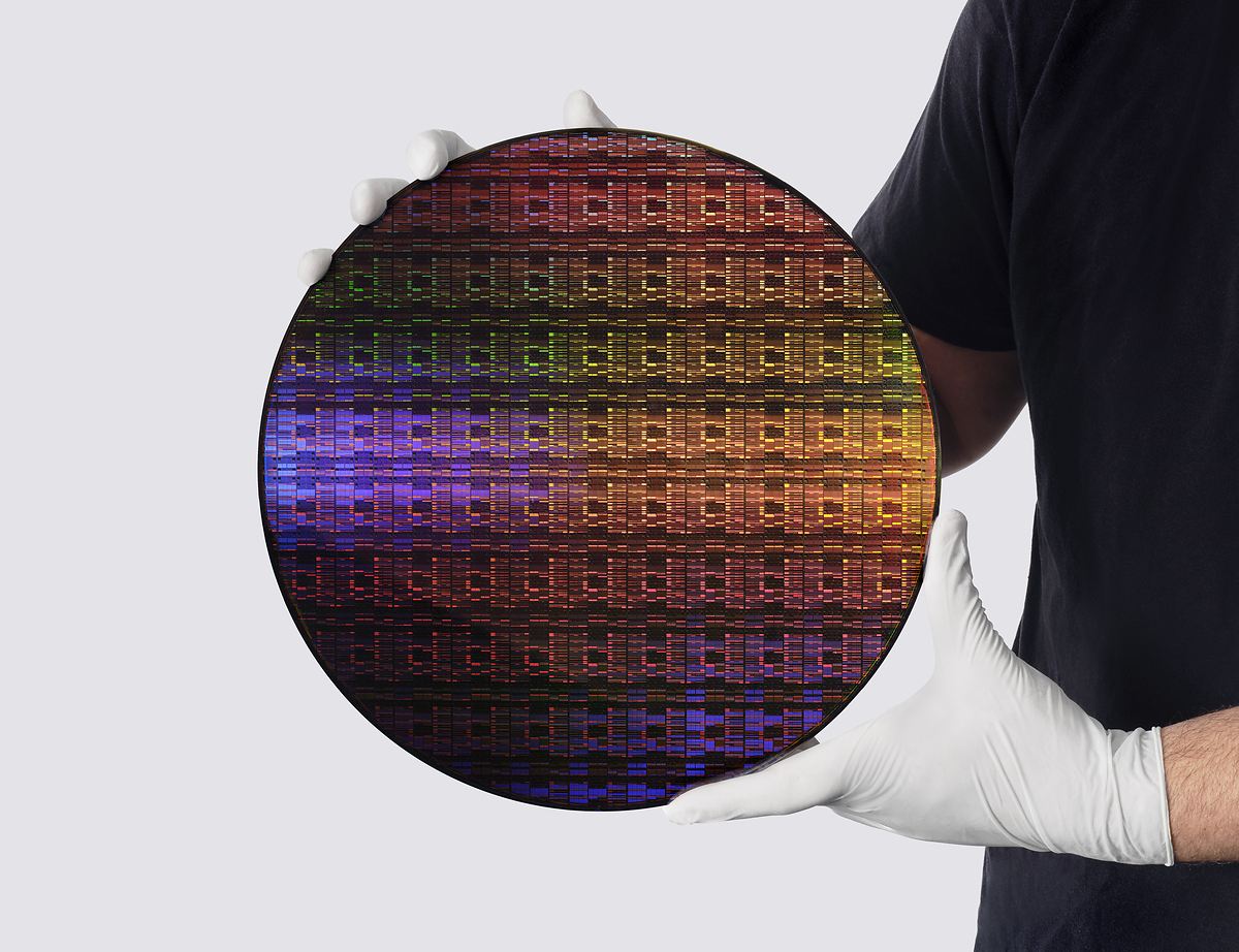
NEW YORK — In a development that rewrites the physical boundaries of semiconductor engineering, IBM has officially debuted the world’s first sub-1 nanometer chip technology, successfully executing at the 0.7-nanometer node. Announced via the IBM Newsroom, this engineering feat defies decades of industry skepticism suggesting that quantum tunneling effects would permanently halt silicon scaling below the 1nm threshold. By introducing a revolutionary "nanostack" 3D chip architecture, Big Blue has not only preserved Moore’s Law but has effectively redefined the future trajectory of global enterprise computing infrastructure.
For institutional investors, enterprise CIOs, and geopolitical strategists tracking the semiconductor space, this breakthrough arrives at a critical juncture. As generative artificial intelligence models demand unprecedented compute density, power grids face severe strain, and data center cooling costs threaten corporate capital expenditure budgets. IBM’s 0.7nm architecture presents a vital lifeline, promising massive power savings and thermal efficiency that could transform cloud compute architecture and recalibrate semiconductor market valuations worldwide.
The Physics of the Breakthrough: Defying Quantum Leakage
Test Our Free AI & Tech Utilities Suite
Calculate LLM API token costs, analyze article dwell-time, or simulate tech DCA returns.
For over fifty years, the semiconductor industry advanced by shrinking transistors down the planar and FinFET scales. However, as nodes approached the 2nm and 1nm thresholds, physics intervened. At this microscopic scale, electrons begin to tunnel through gate barriers unpredictably, causing severe current leakage, thermal throttling, and catastrophic energy loss. Industry consensus long held that silicon was nearing its terminal limit.
IBM’s research and development teams shattered this barrier by abandoning traditional two-dimensional scaling limits. The newly unveiled 0.7nm technology relies on a proprietary "nanostack" 3D architecture. Instead of laying transistors flat or relying solely on vertical nanosheets, IBM vertically integrates the channel layers, optimizing current flow while strictly isolating quantum interference. This structural leap drastically reduces parasitic capacitance and lowers operational voltage requirements without sacrificing switching speed.
From an enterprise ROI perspective, this translates directly into unprecedented transistor density. More compute power packed into a smaller surface area means hyperscalers can process denser neural networks with a fraction of the physical hardware footprint, lowering both initial capital expenditure and ongoing operational expenditure.
Verified Data & Metrics Breakdown

| Metric / Parameter | Legacy 2nm Node Generation | IBM Sub-1nm (0.7nm) Node | Strategic Impact |
|---|---|---|---|
| Node Feature Size | ~2.0 Nanometers | 0.7 Nanometers (Sub-1nm) | Pushes past theoretical quantum limits |
| Architecture Type | Standard FinFET / Early Nanosheet | Proprietary "Nanostack" 3D | Optimizes vertical current flow & density |
| Primary Target Application | General Consumer & Mobile SoC | Enterprise AI & Hyper-scale Cloud | Unlocks massive power savings for LLMs |
| Leakage Mitigation | High tunneling at sub-2nm | Advanced Quantum Barrier Isolation | Drastic reduction in thermal dissipation |
Industry & Market Implications: Winners, Losers, and Economic Shifts
The introduction of IBM’s 0.7nm technology sends shockwaves through the global semiconductor value chain, triggering strategic evaluations across multiple sectors:
- Hyperscale Cloud Providers & AI Giants: Companies spending billions annually on electricity to power massive LLM training clusters stand to capture immediate bottom-line relief. The drastic power savings unlocked by the nanostack architecture directly address the looming grid capacity crisis facing AI data centers.
- Foundry Ecosystem & Capital Allocation: While IBM historically licenses its foundational research rather than operating high-volume consumer foundries directly, this milestone places intense competitive pressure on manufacturing giants like TSMC, Samsung, and Intel to accelerate their own sub-1nm roadmaps. Expect a wave of strategic R&D capital reallocation.
- Semiconductor Equipment Manufacturers: Lithography and etching equipment providers face both immense opportunity and rigorous demand to engineer tools capable of achieving sub-nanometer precision at commercial manufacturing scale.
Regulatory compliance and geopolitical supply chain security will also play a pivotal role. As nodes shrink past 1nm, national security implications surrounding advanced fabrication IP will intensify, prompting tighter regulatory oversight on cross-border technology transfers.
People Also Ask (Frequently Asked Questions)
What is IBM’s sub-1 nanometer chip technology?
IBM's sub-1 nanometer chip technology is a breakthrough semiconductor architecture operating at the 0.7-nanometer node. Utilizing a proprietary "nanostack" 3D design, it overcomes traditional quantum tunneling limitations to deliver massive transistor density and unprecedented power efficiency.
How does the "nanostack" 3D architecture work?
Unlike traditional planar or early FinFET designs where transistors are laid out in two dimensions or simple vertical sheets, IBM's nanostack architecture vertically integrates circuit layers. This optimizes electron flow, prevents current leakage, and drastically cuts thermal waste at sub-1nm scales.
What are the primary benefits for artificial intelligence (AI) applications?
The 0.7nm chips unlock massive power savings critical for enterprise AI workloads. By reducing thermal dissipation and energy consumption per calculation, cloud providers can scale LLM training and inference infrastructures without hitting severe electrical grid or cooling bottlenecks.
When will IBM's 0.7nm chips be commercially available?
While IBM has successfully debuted the technology at the research and development level, commercial fabrication scaling typically requires years of ecosystem tooling refinement. Foundries and enterprise partners will gradually integrate these principles into production pipelines over the latter half of the decade.
Future Outlook: What Comes Next
As IBM transitions this research from laboratory validation to ecosystem commercialization, financial markets and engineering groups will monitor several key milestones. The primary focus shifts toward manufacturing yield optimization, lithographic tool compatibility, and partnership announcements with major foundry operators.
Ultimately, IBM’s successful debut of the 0.7nm sub-1 nanometer chip proves that silicon has not reached its final chapter. By successfully circumventing the physics of quantum leakage through innovative 3D architecture, IBM has established a new benchmark for enterprise compute efficiency—securing its position at the vanguard of the next industrial revolution.