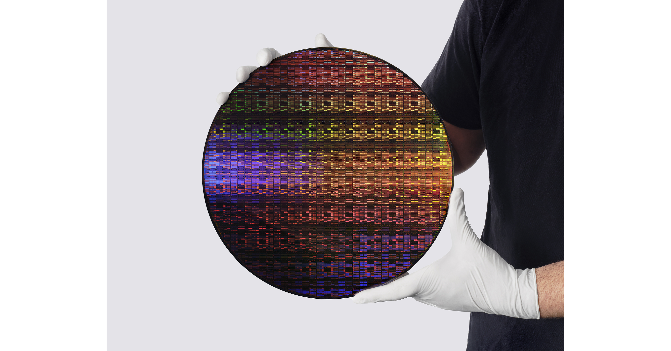
NEW YORK — In what industry veterans are calling the most significant hardware breakthrough of the decade, International Business Machines (IBM) has officially unveiled the world’s first sub-1 nanometer chip technology. Announced today from the company's global newsroom, the landmark engineering feat defies traditional physical limits that have haunted semiconductor manufacturers for years, opening an unprecedented frontier for high-performance computing and energy-efficient artificial intelligence.
The announcement marks a watershed moment for the global technology sector. As generative AI models swell to trillions of parameters and data center power grids face critical capacity bottlenecks, IBM’s new architecture arrives precisely when the industry desperately requires a paradigm shift. By crossing the sub-1 nanometer threshold, Big Blue has proven that Moore’s Law is not dead—it has simply evolved.
Engineering the Impossible: The "Nanostack" 3D Architecture
For decades, semiconductor scaling relied on shrinking transistors horizontally across a silicon wafer. As manufacturers approached the atomic scale, however, quantum tunneling and severe heat dissipation threatened to bring progress to a grinding halt. IBM circumvented these fundamental physics barriers by abandoning traditional two-dimensional scaling entirely.
The secret behind the new processor is IBM’s revolutionary “nanostack” 3D chip architecture. Instead of placing transistors side-by-side, the proprietary design vertically integrates atomic-scale channels. This vertical stacking allows current to flow seamlessly through multiple tiers, drastically minimizing signal latency while maximizing the physical density of the silicon real estate.
According to primary wire disclosures from IBM, the new sub-1 nm chip packs nearly 100 billion transistors onto a piece of silicon no larger than a human fingernail. This staggering density shatters previous benchmarks, offering a glimpse into a future where pocket-sized devices possess the computing power of today's massive enterprise supercomputers.
Unlocking Massive Power Savings for AI Applications

While raw computing power is impressive, the true commercial genius of IBM’s latest breakthrough lies in its unprecedented energy efficiency. Artificial intelligence workloads are notoriously power-hungry, placing an immense financial and environmental burden on cloud providers and enterprise data centers worldwide.
IBM’s newest chip architecture is engineered specifically to alleviate this friction point. Early benchmark indicators suggest the sub-1 nanometer design could unlock massive power savings for AI applications, slashing energy consumption per inference cycle by a double-digit margin compared to current 2nm and 3nm generations.
- Unprecedented Density: Nearly 100 billion transistors packed onto a fingernail-sized footprint.
- Energy Efficiency: Dramatically reduced power consumption designed to curb skyrocketing data center electricity demands.
- Thermal Management: Innovative 3D vertical heat dissipation prevents the thermal throttling common in dense microprocessors.
- AI Acceleration: Native optimization for large-scale machine learning, deep neural networks, and real-time generative models.
“IBM’s latest chip breakthrough marks a landmark moment in the history of computing,” noted senior hardware analysts following the global briefing. “By solving the sub-1 nanometer riddle, they have effectively rewritten the roadmap for the entire semiconductor supply chain, putting immense pressure on competitors like TSMC, Intel, and Samsung to accelerate their own post-nanometer pipelines.”
At a Glance: IBM Sub-1nm vs. Current Industry Standards
| Feature / Metric | Current Industry Standard (3nm) | IBM Sub-1 Nanometer Technology |
|---|---|---|
| Node Architecture | Modified FinFET / 2D Gate-All-Around | Proprietary "Nanostack" 3D Architecture |
| Transistor Density | ~30 to 50 Billion per chip | Nearly 100 Billion per fingernail-sized chip |
| Primary Target | Consumer mobile & general enterprise | Hyperscale AI, Quantum-adjacent workloads |
| Energy Efficiency | Baseline standard | Massive power savings for heavy AI inference |
The Road Ahead: Commercialization and Industry Impact
Following this monumental unveiling, attention immediately turns to commercialization timelines and manufacturing feasibility. Scaling a laboratory breakthrough to mass production at atomic dimensions is an exceptionally complex endeavor. IBM has indicated it will leverage strategic foundry partnerships to transition the nanostack architecture from experimental wafers to high-yield commercial production lines over the next few years.
For enterprise CIOs, cloud architects, and AI developers, the message is clear: hardware constraints that once threatened to cap the growth of artificial intelligence are officially being dismantled. As these sub-1 nanometer chips transition from cleanrooms to data centers, the global tech ecosystem stands on the brink of an entirely new era of hyper-efficient, high-velocity intelligence.
Frequently Asked Questions
What makes IBM's sub-1 nanometer chip different from existing 3nm chips?
Unlike traditional chips that rely on horizontal scaling, IBM’s sub-1 nm breakthrough utilizes a revolutionary "nanostack" 3D architecture. This allows nearly 100 billion transistors to be vertically integrated onto a fingernail-sized piece of silicon, vastly improving performance while overcoming the atomic leakage barriers of older designs.
When will these sub-1 nanometer chips be available commercially?
While IBM has successfully debuted the underlying technology, commercial manufacturing and foundry integration will roll out over the next few years. The primary focus initially will be powering hyperscale enterprise data centers and heavy artificial intelligence workloads.