Quantum Computing’s Silicon Pivot: Imec Fabricates First High-NA EUV Qubit Device, Merging Quantum Hardware With AI Chip Foundries
Executive Takeaways
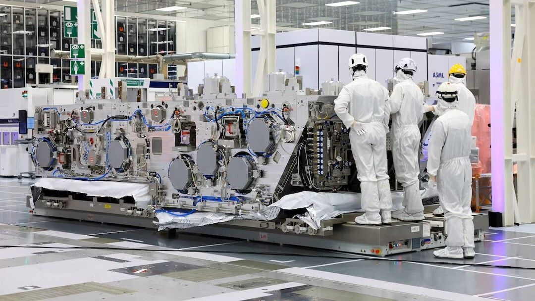
- Industrial Convergence: Belgian nanoelectronics hub imec has successfully fabricated the world's first gate-defined silicon quantum dot qubit device using 0.55 High-Numerical Aperture (High-NA) Extreme Ultraviolet (EUV) lithography on a standard 300mm pilot line.
- Roadmap Compression: The breakthrough tethers quantum hardware manufacturing directly to the semiconductor industry’s leading-edge transistor roadmap (A14/A10 sub-2nm nodes), potentially shaving five to seven years off the timeline toward fault-tolerant, million-qubit systems.
- CapEx Amortization: Utilizing ASML’s $380-million-plus Twinscan EXE lithography systems enables global foundries to amortize advanced lithography infrastructure across high-margin enterprise AI accelerators and nascent quantum processing units (QPUs).
- The Scaling Dilemma Solved: High-NA EUV eliminates the primary bottleneck of silicon spin qubits—the extreme dimensional variance and low throughput of laboratory-scale electron-beam lithography—yielding sub-nanometer critical dimension (CD) uniformity across entire 300mm wafers.
The Cleanroom Breakthrough: Industrializing the Quantum Dot
For more than two decades, quantum computing has occupied an uncomfortable industrial limbo. While classical microelectronics advanced via the predictable, high-yield cadence of Moore’s Law, quantum processing units (QPUs) remained largely handcrafted artifacts. Most quantum architectures—from superconducting circuits with their millimeter-scale transmon footprints to trapped-ion vacuum chambers—fundamentally conflict with the geometric economics of modern semiconductor fabrication plants (fabs).
This week, Belgian research institute imec altered that trajectory. Operating out of its advanced 300mm pilot line in Leuven, imec engineers unveiled what they verified as the world’s first functional quantum dot qubit device patterned using 0.55 High-NA EUV lithography. The achievement confirms that silicon spin qubits—which represent quantum information using the spin state of single electrons trapped in microscopic electrostatic potential wells—can be manufactured using the exact tools, chemistries, and yield-management strategies earmarked for the next generation of generative AI accelerators.
Silicon spin qubits have long possessed the theoretical advantage of extreme density. Unlike superconducting qubits, which measure hundreds of micrometers across, a gate-defined quantum dot measures roughly 20 to 30 nanometers—virtually identical in scale to a modern gate-all-around (GAA) nanosheet transistor. However, this microscopic advantage has historically been an engineering curse. To control single-electron confinement, gate pitches must fall below 30 nanometers with atomic-level placement precision. Until now, producing these features required academic-grade electron-beam (e-beam) lithography: an agonizingly slow, single-beam writing process incapable of commercial scaling and plagued by qubit-to-qubit device variation.
The Physics of High-NA EUV: Sub-Nanometer Control at 13.5 Nanometers
Imec’s transition to High-NA EUV represents a triumph of lithographic physics over quantum mechanical decoherence. ASML’s Twinscan EXE:5000 and EXE:5200 lithography systems project light at an extreme ultraviolet wavelength of 13.5nm through an anamorphic lens configuration with a 0.55 numerical aperture, up from the 0.33 NA found on standard EUV systems. This optical architecture yields an 8nm half-pitch resolution in a single exposure, radically eliminating the need for complex, defect-prone multi-patterning litho-etch cycles.
In quantum dot fabrication, variability is the primary driver of device failure. An interface deviation of just two silicon atoms at the dielectric boundary shifts the chemical potential of the dot, causing unpredictable electrostatic landscapes that destroy quantum coherence ($T_2^*$) and require individual, unscalable gate voltage tuning. Imec’s demonstration proved that High-NA EUV’s depth-of-focus and line-edge roughness (LER) controls can achieve sub-0.5nm critical dimension uniformity across a 300mm wafer surface.
By pairing High-NA EUV with isotopically purified Silicon-28 ($^{28}\text{Si}$) epitaxial substrates—which strip out the nuclear spin noise found in natural silicon—imec has engineered a path toward gate-defined quantum structures with uniform barrier-gate pitches, low parasitic capacitance, and the structural repeatability necessary to run surface code quantum error correction.
Comparative Analysis: Lithographic Regimes for Quantum Device Fabrication
The transition from experimental laboratory patterning to industrial High-NA EUV fundamentally alters the physics, throughput, and unit economics of quantum chip fabrication.
| Metric / Specification | Academic Electron-Beam (E-Beam) | Standard 0.33 NA Low-NA EUV | Imec 0.55 High-NA EUV (300mm) |
|---|---|---|---|
| Optical Resolution Limit | ~5 nm to 10 nm | ~13 nm (single exposure) | < 8 nm (single exposure) |
| Wafer Throughput | < 0.1 wafers / day | 160–200 wafers / hour | 185–220 wafers / hour |
| Critical Dimension Uniformity (3σ) | ± 2.5 nm to 4.0 nm | ± 1.1 nm to 1.5 nm | < ± 0.5 nm |
| Gate-to-Gate Pitch | Variable (Stitching errors) | 30 nm – 36 nm (Multi-patterning required) | < 24 nm (Single exposure) |
| Interfacial Defect Density | High ( Loading article content... |
Low ( Loading article content... |
Ultra-Low ( Loading article content... |
| Economic Scaling Horizon | Bespoke R&D only | Intermediate / High defect risk | Commercial Foundries (Intel, TSMC, Samsung) |
Industry & Market Implications: The Foundry Shakeup
Imec’s milestone delivers massive economic ramifications across the global semiconductor and enterprise compute landscape. The primary beneficiaries are the leading-edge logic foundries—specifically Intel Foundry, TSMC, and Samsung Electronics—alongside optical monopoly ASML.
1. Capital Allocation & Fab Multiples
Leading-edge foundries are committing tens of billions of dollars in capital expenditure (CapEx) to integrate High-NA EUV into their 1.4nm (Intel 14A) and 2nm-class production lines. Until now, this expenditure was underwritten solely by high-performance enterprise AI silicon, sovereign high-performance computing (HPC) grants, and premium mobile APUs. Imec has demonstrated that this exact CapEx deployment directly serves the future quantum roadmap. Foundries can now cross-amortize lithography tools across AI and quantum lines, dramatically lowering the marginal cost of building commercial-grade QPUs.
2. Competitive Pressures on Superconducting and Trapped-Ion Pure-Plays
Public and venture-backed quantum pure-plays utilizing alternative modalities—such as IBM, Rigetti Computing, IonQ, and Quantinuum—face a sudden recalibration of their long-term cost structures. Superconducting qubits require vast cryogenic footprints, dilution refrigerators the size of industrial storage units, and complex RF cabling to service modest qubit counts. Silicon spin qubits, by contrast, operate at slightly elevated cryogenic temperatures (1 to 4 Kelvin vs. millikelvin levels), enabling co-integration with classical control electronics via advanced Cryo-CMOS on the same silicon die.
If silicon spin qubits can achieve two-qubit gate fidelities exceeding 99.9% at commercial scale, the pure-play hardware developers risk competing against the multi-billion-dollar manufacturing efficiencies of the commercial semiconductor foundry ecosystem.
3. Geopolitical and Export Control Regimes
High-NA EUV tools are strictly controlled dual-use technologies, barred from export to China and other adversarial nations under trilateral export controls between the United States, the Netherlands, and Japan. By anchoring quantum hardware production to High-NA EUV, the Western semiconductor alliance effectively extends its geopolitical moat. Any nation locked out of High-NA EUV is now not only barred from competing in leading-edge AI compute infrastructure, but also systematically constrained from scaling silicon-based fault-tolerant quantum computers.
Frequently Asked Questions (People Also Ask)
How does High-NA EUV lithography accelerate the path to commercial quantum computing?
High-NA EUV lithography provides sub-8nm optical resolution and sub-nanometer critical dimension uniformity on standard 300mm silicon wafers. Historically, silicon quantum dot qubits were patterned using slow, non-uniform electron-beam lithography, which caused high device-to-device variability and low manufacturing yields. High-NA EUV enables foundries to mass-produce billions of atomically precise gate electrodes with exceptional yield, compressing the commercial transition from small-scale lab prototypes to million-qubit processors.
Why are silicon spin qubits favored over superconducting qubits for mass fabrication?
Silicon spin qubits have a physical footprint roughly 10,000 times smaller than superconducting transmons (nanometers versus hundreds of micrometers). Because their operational structures mirror gate-all-around (GAA) silicon transistors, they can be fabricated in standard commercial fabs using existing CMOS toolsets. Furthermore, silicon spin qubits can be monolithically or heterogeneously integrated with classical Cryo-CMOS control circuits on the same silicon substrate, solving the severe input/output (I/O) wiring bottleneck that limits alternative quantum modalities.
What are the economic and CapEx implications for semiconductor foundries?
ASML's High-NA EUV systems cost in excess of $380 million per unit. Demonstrating that these machines can manufacture quantum processors allows foundries (such as Intel, TSMC, and Samsung) to leverage their multi-billion-dollar capital investments across both enterprise AI accelerators and future quantum computing hardware. This dual-use capability improves overall capital efficiency, accelerates tool depreciation recovery, and lowers the barrier to entry for commercial quantum silicon production.
What technical hurdles remain before commercial fault-tolerant quantum processors arrive?
While lithographic uniformity is now solvable via High-NA EUV, significant engineering hurdles remain. Foundries must still master the integration of isotopic Silicon-28 without introducing interface stress, achieve two-qubit gate fidelities consistently above the 99.9% fault-tolerance threshold across millions of contiguous dots, and develop ultra-low-power cryogenic interconnects capable of reading and routing millions of analog quantum signals without introducing thermal back-action into the dilution refrigerator.
Strategic Horizon: The Roadmap to 2030
Imec’s milestone is not merely an academic validation; it marks the commercialization baseline for quantum hardware. Over the next 24 to 36 months, the focus in Leuven and across allied foundry partner labs will shift from single-device proof-of-concept to scaling linear and two-dimensional crossbar arrays to hundreds, and eventually thousands, of coupled qubits.
Between 2027 and 2029, investors and enterprise IT strategists should watch for the integration of Cryo-CMOS control logic directly alongside High-NA EUV-patterned qubit arrays using 3D heterogeneous stacking technologies like wafer-to-wafer hybrid bonding. Once classical control chips and quantum dot arrays can be bonded within a unified microelectronics package, the path toward a fault-tolerant, commercial quantum computing appliance will no longer run through bespoke physics laboratories. It will run through the world’s most advanced commercial chip foundries.