Inside New Delhi’s $15 Billion Silicon Gamble: How India Is Rewiring the Global Semiconductor Map
NEW DELHI & BENGALURU — As the Union Cabinet greenlights two landmark fabrication facilities, global capital, geopolitical urgency, and aggressive state subsidies collide in a high-stakes bid to break East Asia’s chip monopoly.
Executive Takeaways
- Catalytic Cabinet Approvals: On May 5, 2026, India’s Union Cabinet formally ratified two next-generation semiconductor ventures, allocating an incremental $3.8 billion in targeted state fiscal support under the expanded India Semiconductor Mission (ISM 2.0).
- Strategic Node Diversification: New Delhi has pivoted beyond mature legacy nodes (28nm–90nm), structuring financial incentives toward advanced compound semiconductors, power electronics (SiC/GaN), and cutting-edge 2.5D/3D packaging facilities designed to feed sovereign AI compute clusters.
- Capital Allocation Arbitrage: The 50% central fiscal parity scheme—coupled with 20% to 25% state-level matching top-ups—creates an unprecedented 70% to 75% public underwriting of baseline capital expenditure (CAPEX), fundamentally altering enterprise ROI calculations for multinational foundries.
- Structural Chokepoints: Despite robust fiscal liquidity, yield-rate optimization, reliable high-voltage grid stability, and localized supply chains for specialty gases and ultra-pure water (UPW) remain severe execution risks through 2028.
The New Delhi Gambit: Escalating from Assembly to Core Silicon
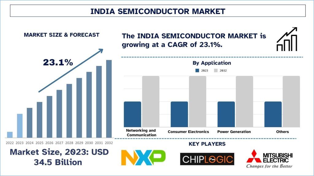
For decades, the global semiconductor supply chain viewed the Indian subcontinent through a paradoxical lens: indispensable for design engineering, yet nonexistent in physical fabrication. Nearly 20% of the world’s top chip design talent sits in Bengaluru, Hyderabad, and Noida, optimizing complex layout architectures for Nvidia, Qualcomm, and Intel. Yet, every commercial wafer designed within India’s borders was exported to Taiwan, South Korea, or mainland China for front-end fabrication.
That structural asymmetry is undergoing aggressive industrial realignments. On May 5, 2026, the Union Cabinet approved two high-profile semiconductor proposals, solidifying the second chapter of the ambitious $10-billion-plus India Semiconductor Mission. This executive action marks a deliberate operational pivot from low-complexity Outsourced Semiconductor Assembly and Test (OSAT) units toward specialized analog fabs and advanced wafer packaging ecosystems.
The catalytic nature of these approvals addresses two critical macroeconomic priorities: national security imperatives surrounding silicon sovereignty and enterprise-level supply chain de-risking under the "China+1" corporate doctrine. With global market liquidity tightening and valuation multiples for industrial technology firms demanding disciplined balance sheet management, India has weaponized central and state treasury balance sheets to subsidize private enterprise risk.
Deconstructing the May 5 Approvals: Capital Allocation and Strategic Alignment
The two recently sanctioned projects reflect a nuanced shift in New Delhi's industrial policy. Rather than attempting a capital-incinerating leap directly into sub-3nm extreme ultraviolet (EUV) lithography—a domain fiercely defended by TSMC, Samsung, and Intel—India’s Ministry of Electronics and Information Technology (MeitY) is methodically capturing automotive, industrial IoT, and power-grid verticals.
The first approved project is an integrated Compound Semiconductor Wafer Fab, engineered explicitly for Silicon Carbide (SiC) and Gallium Nitride (GaN) substrates. Supported by a domestic industrial conglomerate in joint venture with a leading European automotive chipmaker, the facility will supply traction inverters, fast-charging infrastructure, and renewable energy grids. SiC and GaN technologies bypass the cutthroat photolithography race, relying instead on specialized material sciences where margin compression is lower and enterprise ROI horizons are faster.
The second approval establishes an Advanced Substrate and 2.5D/3D Heterogeneous Integration packaging hub. As traditional Moore’s Law scaling confronts thermal and quantum physical ceilings, high-performance computing (HPC) and sovereign cloud compute architecture increasingly rely on advanced multi-die packaging. By housing high-density wafer-level chip-scale packaging (WLCSP) domestically, India guarantees that compute modules driving national AI initiatives are shielded from East Asian maritime disruptions.
These initiatives integrate seamlessly with ongoing foundational projects: the Tata Electronics–Powerchip Semiconductor Manufacturing Corp (PSMC) 300mm wafer fab in Dholera, Gujarat (targeting 28nm, 40nm, and 91nm nodes), and the advanced packaging facilities commissioned by Micron Technology, CG Power-Renesas, and Kaynes Semicon.
Data Sheet: Capital Expenditure, Capacity, and Strategic Nodes
The economic profile of India's current semiconductor pipeline reveals an aggressive distribution of capital expenditure across front-end foundries, specialty fabs, and backend packaging architectures:
| Project / Lead Entity | Joint Venture / Tech Partner | Projected CAPEX (USD) | Target Node / Specialization | Operational Horizon | Fiscal Subsidy Underwrite |
|---|---|---|---|---|---|
| Tata Electronics (Dholera, Gujarat) | PSMC (Taiwan) | $11.0 Billion | 28nm, 40nm, 91nm Logic & Mixed-Signal | Q4 2026 – Q1 2027 | 50% Central + 20% State matching |
| Micron Technology (Sanand, Gujarat) | Wholly Owned (ATMP) | $2.75 Billion | DRAM & NAND Flash Packaging | Phased Operational Ramp (2025–2026) | 50% Central + 20% State matching |
| CG Power – Renesas (Sanand, Gujarat) | Renesas Electronics (Japan) / Stars Micro | $920 Million | Legacy Wirebond, Flip-Chip OSAT | H2 2026 | 50% Central + 20% State matching |
| Approved Venture A (May 5, 2026) | European Power Semi Consortium | $2.10 Billion | Silicon Carbide (SiC) / GaN Wafer Fab | H1 2028 | 50% Central + 25% State matching |
| Approved Venture B (May 5, 2026) | Domestic Tech Tier-1 / OSAT Specialist | $1.70 Billion | Advanced Substrates, 2.5D/3D Packaging | Late 2027 | 50% Central + 25% State matching |
Structural Friction: The Engineering and Infrastructure Bottlenecks
While sovereign balance sheets can underwrite capital acquisition, physical fabrication plants ("fabs") are unforgiving environments governed by chemical precision, uninterrupted utility supply, and rigorous regulatory compliance. Industry executives caution that capital allocation is simply the first hurdle.
1. Ultra-Pure Water (UPW) and Chemical Supply Chains
A standard 300mm front-end wafer fabrication plant consumes between 3 to 5 million gallons of Ultra-Pure Water daily. UPW requires multi-stage filtration to parts-per-billion or parts-per-trillion contamination thresholds. In semi-arid manufacturing belts like Gujarat, industrial developers have had to deploy massive desalination infrastructures and dedicated recycling facilities to guarantee water uptime. Furthermore, raw chemical supply chains—ranging from electronic-grade hydrogen fluoride to isopropyl alcohol—remain heavily reliant on imports from Japan, Germany, and the United States, creating an acute supply chain vulnerability.
2. Power Quality and Grid Volatility
Unlike standard industrial manufacturing, semiconductor fabs cannot tolerate a voltage fluctuation lasting a fraction of a second; a transient millisecond drop on an electrical feeder can ruin an entire production batch of wafers, generating tens of millions of dollars in scrapped work-in-progress. State power distribution companies (DISCOMs) are constructing triply redundant 400kV transmission lines backed by industrial-grade uninterruptible power supply (UPS) banks, but long-term operational resilience under extreme summer peak demands has yet to be battle-tested.
3. Yield-Rate Optimization and Workforce Specialization
Yield rate—the percentage of non-defective dies per wafer—governs the line between enterprise profitability and rapid insolvency. Achieving an 85%+ commercial yield requires years of engineering intuition on the fab floor. While India commands unmatched digital software design talent, it faces a localized deficit of cleanroom technicians, vacuum maintenance engineers, and process control metallurgists. New Delhi’s fast-tracked semiconductor university curricula and technical institution tie-ups are working to compress a multi-decade workforce maturation cycle into a five-year deployment window.
Market Winners, Structural Losers, and Institutional Impact
The systematic reorganization of India’s semiconductor vertical is forging clear divisions across global enterprise landscapes:
- Clear Winners:
- Domestic Conglomerates: Groups such as Tata, Murugappa, and Larsen & Toubro are securing critical first-mover advantages, vertically integrating chip fabrication directly into their own automotive, aerospace, and power transmission conglomerates.
- Global Equipment Suppliers: Capital goods manufacturers including Applied Materials, Lam Research, ASML, and Tokyo Electron are realizing windfall revenue streams, selling legacy and specialized tooling suites backed by government-funded letters of credit.
- Global Fabless OEMs: Automotive and industrial IoT manufacturers gain critical geographic risk mitigation, reducing single-source dependency on Taiwan-strait supply corridors.
- Challenged Players:
- Pure-Play OSATs in East Asia: Traditional packaging houses in Malaysia, the Philippines, and mainland China face margin compression as low-to-mid complexity packaging volume is retained within the Indian domestic market to offset import tariffs.
- Sub-Scale Domestic Manufacturers: Companies attempting chip-making without massive conglomerate backing or institutional joint ventures face acute capital starvation, as both central authorities and institutional private equity gravitate exclusively toward projects requiring multi-billion-dollar commitments.
Frequently Asked Questions (People Also Ask)
Why is the Indian government subsidizing up to 70% of semiconductor fab costs?
Front-end semiconductor fabrication requires astronomical CAPEX, often exceeding $10 billion for a commercial-scale logic plant, paired with prolonged payback periods and high cyclical volatility. To persuade risk-averse multinationals to locate assets outside established semiconductor ecosystems (such as Taiwan or South Korea), the central government covers 50% of the project cost on an equal pari-passu basis, while state governments offer top-ups of 20% to 25%. This aggressive fiscal subsidy radically lowers the baseline cost of capital and accelerates enterprise ROI.
Is India competing directly with TSMC on cutting-edge 2nm and 3nm chips?
No. India’s strategic road map purposely avoids the direct, cost-prohibitive sub-5nm race dominated by TSMC, Intel, and Samsung. Instead, India is deploying capital into legacy logic nodes (28nm to 90nm), compound semiconductors (Silicon Carbide and Gallium Nitride), and advanced packaging. These nodes represent over 50% of global industrial, automotive, and consumer electronics demand, securing profitability and domestic supply chain autonomy without the immense capital risks of EUV lithography.
What role does the 'China+1' strategy play in India’s semiconductor rise?
Geopolitical friction, cross-strait operational vulnerabilities, and Western export controls on semiconductor equipment have forced global fabless brands and automotive manufacturers to establish alternative sourcing lines. India provides structural stability: deep software-engineering talent, a massive and growing internal consumer market, sovereign legal protections, and extensive fiscal backing, making it a premier candidate for long-term supply chain de-risking.
How does India plan to solve the semiconductor talent shortage?
While India has over 100,000 design engineers working for multinational semiconductor design centers, cleanroom and physical fab technicians are scarce. MeitY has launched specialized semiconductor curricula across more than 300 universities and engineering institutions, partnering with leading equipment manufacturers to deploy standardized training toolkits, cleanroom simulator labs, and international exchange programs with institutions in Taiwan, Japan, and the United States.
Future Outlook: Milestones to Watch (2026–2030)
As the May 5, 2026 cabinet approvals transition from policy blueprints to active civil construction, the global tech industry will be watching key milestone gates. The critical variable across the next 18 months remains the successful "first-silicon" output from the Dholera and Sanand facilities. Delivering commercial-grade, defect-free silicon on predictable schedules will determine whether global institutional capital continues to flow into India's semiconductor corridors.
The window between 2026 and 2030 will also test the sustainability of state fiscal support. If India's nascent foundries can nurture a localized base of chemical, gas, substrate, and maintenance suppliers, the country will have successfully engineered an indigenous tech ecosystem capable of sustained self-replication. If structural chokepoints stall yield progression, New Delhi will face mounting fiscal pressure over capital expenditure underwriting. For now, the momentum is undeniable: global silicon manufacturing is breaking free of its historic geographic constraints, and India has firmly staked its claim.