Executive Takeaways
- Microarchitectural Milestone: IBM Research successfully prototyped the world’s first 2-nanometer (nm) nanosheet semiconductor test chip, packing a staggering 50 billion transistors onto a fingernail-sized footprint.
- Economic & Performance Delta: The architecture delivers up to a 45% performance increase or a 75% energy reduction compared to prevailing 7nm-node enterprise chips, fundamentally altering enterprise ROI calculations for hyper-scale data centers.
- Supply Chain & Capital Shifts: The breakthrough arrives at a critical juncture of global semiconductor supply chain vulnerability, injecting fresh strategic leverage into American and Western capital allocation for domestic advanced manufacturing infrastructure.
- Commercialization Timeline: While initial laboratory validation is complete, scaling these fabrication techniques to high-volume foundry production remains a multi-year risk-mitigation challenge for industry partners like Samsung and Intel.
NEW YORK — In the high-stakes theater of global semiconductor dominance, scale is measured not merely in billions of dollars, but in atomic fractions. On May 6, 2021, International Business Machines (IBM) Corporation crossed a formidable technological Rubicon. At its Albany NanoTech Complex, IBM Research unveiled the world’s first functioning 2nm semiconductor test chip, housing 50 billion microscopic switches onto a die no larger than a fingernail.
For decades, Moore’s Law—the empirical observation that the number of transistors on a microchip doubles roughly every two years—has served as the sacred text of the digital economy. Yet, as lithography approached the single-digit nanometer threshold, physical roadblocks multiplied. Quantum tunneling, severe thermal dissipation, and exponential leakage currents threatened to halt progress. IBM’s 2nm announcement did not just bypass these roadblocks; it signaled that silicon scaling still holds untapped reserves of enterprise transformation, cloud compute architecture optimization, and long-term valuation multiples for forward-thinking technology portfolios.
The Anatomy of a Breakthrough: Engineering at the Atomic Scale
Test Our Free AI & Tech Utilities Suite
Calculate LLM API token costs, analyze article dwell-time, or simulate tech DCA returns.
To understand the magnitude of IBM’s May 2021 disclosure, one must examine the physics governing modern microprocessors. As nodes shrink, traditional FinFET (Fin Field-Effect Transistor) architectures run out of geometric headroom. Control over the channel becomes increasingly difficult as gates shrink, leading to uncontrolled current leakage.
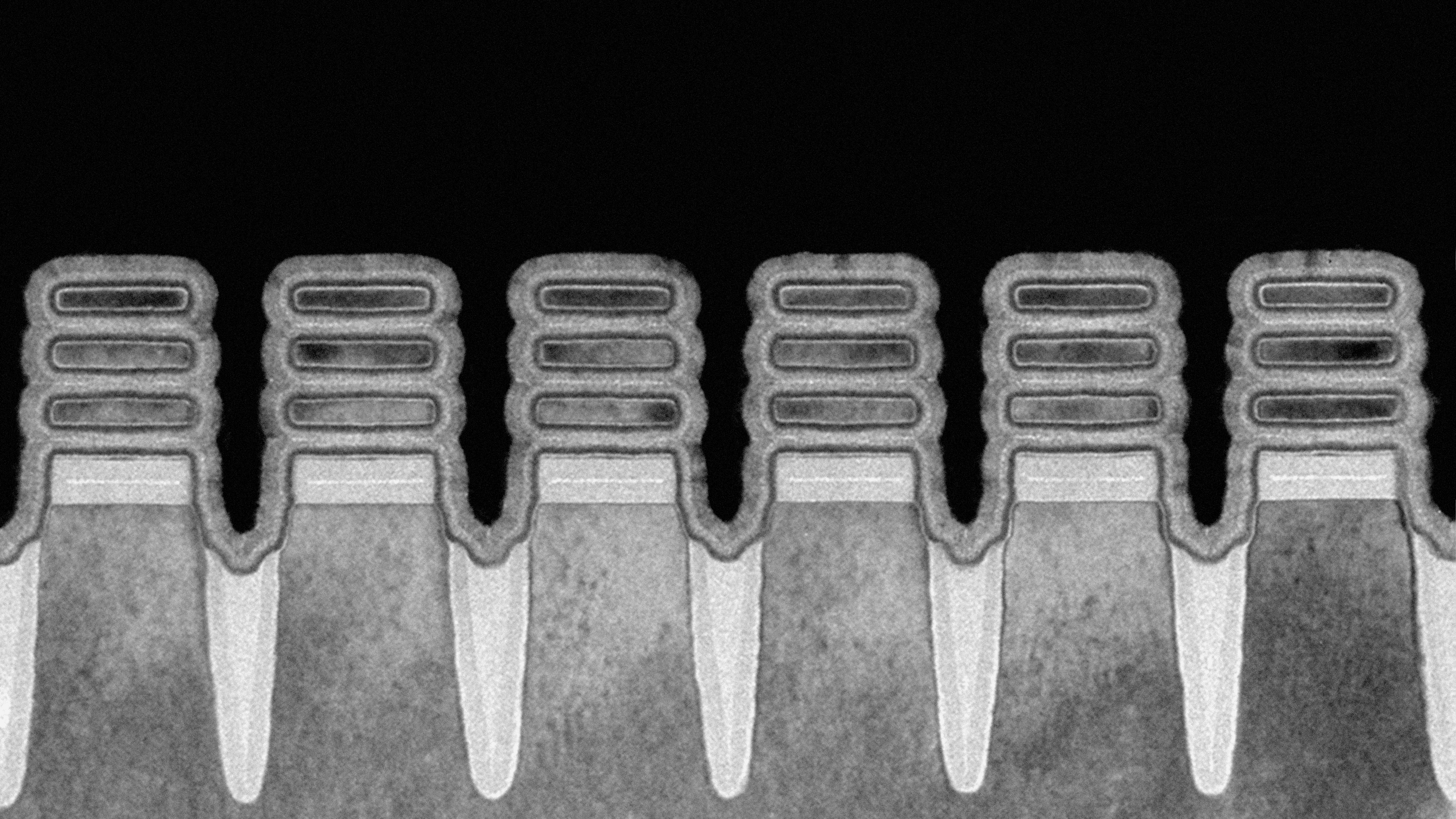
IBM circumvented this physical barrier by pioneering a nanosheet (or gate-all-around, GAA) transistor architecture. Rather than relying on upright fins, IBM’s design stacks horizontal nanosheets of silicon. This configuration allows the gate material to completely wrap around all sides of the channel, maximizing electrostatic control and virtually eliminating current leakage when the switch is in the "off" state.
Within this architectural framework, IBM engineers achieved a density of 50 billion transistors within a 150-square-millimeter footprint. To put this density into perspective, consider the daily operational realities of enterprise IT infrastructure. Data center operators are locked in a relentless battle against escalating power bills and cooling expenditures. According to internal benchmarks released by IBM Research, processors built on this 2nm process technology can achieve:
- A 45% boost in processing performance when operating at the same power level as current 7nm-node mainstream chips.
- A 75% reduction in power consumption when delivering the exact same computational throughput as standard 7nm enterprise processors.
- Extended mobile battery life—potentially quadrupling smartphone longevity between charges, requiring users to plug in only once every four days.
- Accelerated AI workloads, enabling faster natural language processing, real-time edge translation, and complex object detection in autonomous systems without scaling energy footprints.
From a financial perspective, these metrics translate directly into enhanced enterprise ROI. Lower power draw per rack unit allows cloud providers and hyperscalers to drastically reduce infrastructure scaling costs and mitigate regulatory compliance pressures associated with corporate carbon neutrality mandates.
Verified Data & Metrics Breakdown

A rigorous comparative analysis of historical and advanced semiconductor milestones underscores the architectural leap represented by IBM’s 2nm test chip:
| Node Generation | Transistor Architecture | Approximate Density | Key Performance / Efficiency Advantage | Primary Market Application |
|---|---|---|---|---|
| 7nm (Baseline) | FinFET | ~100M transistors / mm² | Established high-volume standard for mobile and server CPUs. | Smartphones, standard hyperscale servers. |
| 5nm | Advanced FinFET / Early GAA | ~170M transistors / mm² | ~15% speed increase or 30% power reduction vs. 7nm. | Flagship mobile devices, premium laptops. |
| 2nm (IBM Test Chip) | Multi-Bridge Channel Nanosheet (GAA) | ~333M transistors / mm² (50B on ~150mm²) | +45% performance or -75% power vs. 7nm. | Next-gen AI datacenters, autonomous systems, high-performance computing (HPC). |
Industry & Market Implications: Re-allocating Global Capital and Tech Hegemony
The macroeconomic ramifications of IBM’s breakthrough extend far beyond the laboratory cleanrooms of upstate New York. In May 2021, the global economy was grappling with acute semiconductor shortages, exposing the brittle nature of centralized supply chains concentrated predominantly in East Asia.
By demonstrating that advanced semiconductor research and foundational IP generation remain robust within Western R&D ecosystems, IBM altered the strategic calculus for sovereign governments and multinational conglomerates. Key stakeholders across the economic landscape experienced immediate ramifications:
- Foundry Ecosystems & Manufacturing Partners: While IBM no longer operates high-volume mass-production fabrication plants—having famously divested its semiconductor manufacturing division to GlobalFoundries in 2015—the company licenses its technology to major foundry partners. Manufacturers such as Samsung and Intel have watched closely, incorporating aspects of GAA architecture into their own roadmap strategies to capture future foundry market share.
- Capital Allocation and Venture Liquidity: Venture capital and private equity firms tracking deep-tech infrastructure re-evaluated valuations for enterprise hardware startups. Companies capable of designing accelerators that leverage ultra-dense nodes instantly commanded premium valuation multiples, as institutional investors recognized the insurmountable moat provided by sub-3nm design capabilities.
- Geopolitical Risk Mitigation: With governments in Washington and Brussels injecting hundreds of billions of dollars into domestic semiconductor manufacturing subsidies (such as the legislative precursor to the U.S. CHIPS Act), discoveries like IBM’s 2nm chip provided vital justification for public sector capital allocation, ensuring that national security and critical infrastructure remain anchored to cutting-edge domestic research.
People Also Ask (Frequently Asked Questions)
What makes IBM’s 2nm chip architecture different from current commercial processors?
Unlike traditional FinFET transistors used in 7nm and 5nm chips—which utilize vertical fins to control electrical current—IBM’s 2nm test chip uses a nanosheet (Gate-All-Around or GAA) architecture. This design stacks horizontal ribbons of silicon, allowing the gate to wrap entirely around the channel. This complete enclosure maximizes electrostatic control, drastically reducing current leakage and enabling unprecedented transistor density (50 billion transistors on a fingernail-sized die).
When will 2nm processors become commercially available for enterprise and consumer markets?
Transitioning from a functional laboratory prototype to high-volume foundry manufacturing is an intricate, multi-year engineering undertaking. Following IBM’s May 2021 announcement, industry analysts projected that commercial production and widespread market deployment of 2nm-based chips would ramp up between 2024 and 2025, driven by major fabrication partners integrating IBM’s foundational research into their commercial pipelines.
How does the 2nm milestone impact enterprise data center ROI and sustainability goals?
The 2nm node delivers a 75% reduction in power consumption or a 45% increase in performance compared to 7nm chips. For enterprise data center operators, this efficiency translates directly into lower electricity bills, reduced cooling infrastructure requirements, and a significantly smaller carbon footprint. This directly supports corporate Environmental, Social, and Governance (ESG) mandates while lowering total cost of ownership (TCO) for hyperscale cloud compute architectures.
Does IBM manufacture these 2nm chips themselves?
No. IBM develops foundational semiconductor research and process technology at its Albany NanoTech Complex. Rather than operating mass-production fabrication plants, IBM partners with major global foundries—such as Samsung and Intel—to license and scale these innovations for commercial volume production.
Future Outlook: Navigating the Road to Commercialization
As the semiconductor industry looks past the milestone set in May 2021, the focus shifts squarely from laboratory demonstration to manufacturing yield optimization. Prototyping a single test wafer with 50 billion transistors is a profound scientific victory; ensuring that millions of identical wafers can be produced with defect-free yields on extreme ultraviolet (EUV) lithography systems is an entirely different operational hurdle.
Looking ahead, the market will monitor several critical inflection points:
- EUV Lithography Refinement: The commercialization of 2nm and sub-2nm nodes requires continuous advancement in high-NA (Numerical Aperture) EUV equipment, a capital-intensive domain dominated by Dutch equipment giant ASML.
- Packaging Innovations: As monolithic die scaling faces rising costs, advanced 3D chiplet integration and heterogeneous packaging will work in tandem with 2nm nodes to sustain performance gains.
- Software and Compiler Adaptation: Enterprise software stacks, operating systems, and AI frameworks must be optimized to exploit the unique instruction-level parallelism and low-latency advantages offered by GAA architectures.
Ultimately, IBM’s 2nm test chip announcement stands as a watershed moment in industrial history. It proved premature to write the obituary for physical scaling. For enterprise leaders, CIOs, and institutional investors, the message is unequivocal: the silicon roadmap remains active, and the organizations that align their cloud infrastructure, AI models, and capital expenditure strategies with these emerging node transitions will capture outsized market dominance in the decade ahead.