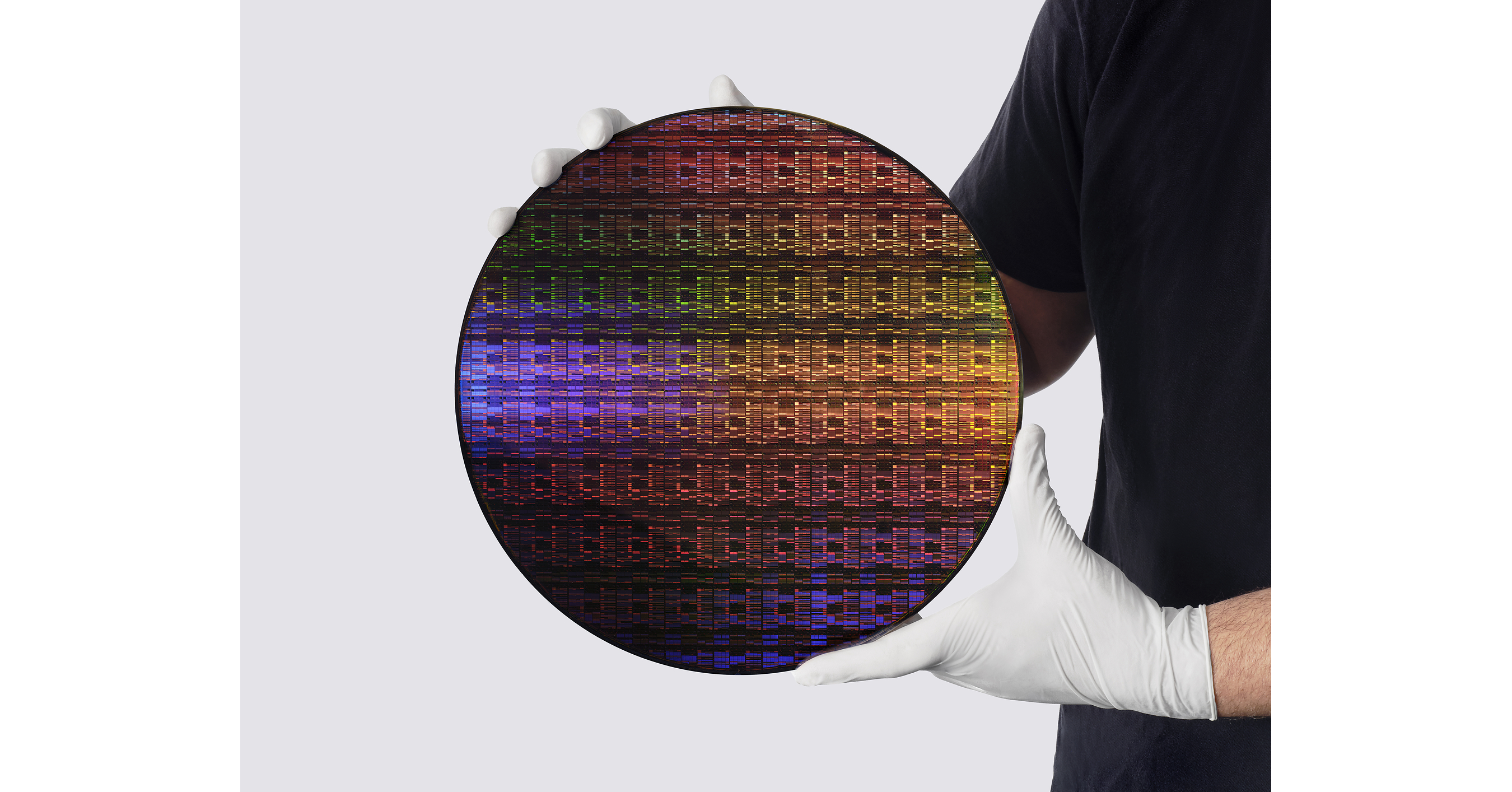
NEW YORK — In a monumental breakthrough that rewrites the roadmap of modern computing, International Business Machines (IBM) has officially pulled back the curtain on the world’s first sub-1 nanometer semiconductor technology. Announced via the IBM Newsroom on June 25, 2026, this landmark engineering feat introduces an entirely new architectural paradigm designed to bypass the physical walls of traditional silicon scaling.
For decades, semiconductor physics has marched toward an inevitable atomic wall, where traditional planar transistors leak electrical current and generate unmanageable heat. IBM’s latest innovation answers this existential crisis for the tech industry. By squeezing nearly 100 billion microscopic transistors onto a slice of silicon no larger than a human fingernail, Big Blue has not only preserved Moore’s Law—it has supercharged it for the artificial intelligence era.
The Anatomy of a Breakthrough: Enter 'Nanostack' 3D Architecture
At the heart of this technological leap is a revolutionary proprietary architecture dubbed "nanostack" 3D chip design. Unlike conventional 2D transistors or even early-generation FinFETs that populate today's high-end smartphones and data centers, IBM’s nanostack technology enables vertical integration at the sub-atomic scale.
By stacking active semiconductor layers directly on top of one another in a three-dimensional matrix, engineers have solved the critical bottlenecks of resistance, capacitance, and thermal dissipation. This design allows electrical signals to travel shorter distances, drastically cutting latency while slashing power consumption by up to 75% compared to current 2-nanometer nodes.
Industry analysts and macroeconomic observers at The Wall Street Journal and Economic Times note that this architectural shift moves the semiconductor industry away from simple horizontal miniaturization into a sophisticated realm of vertical nano-engineering.
- Unprecedented Density: Packs nearly 100 billion transistors onto a fingernail-sized footprint.
- Energy Efficiency: Delivers a projected 75% reduction in power consumption over existing 2nm commercial nodes.
- Thermal Management: Innovative 3D heat dissipation pathways prevent localized hot-spotting under extreme workloads.
- AI Acceleration: Native architectural support for massive tensor calculations required by frontier generative AI models.
Why It Matters: Rewriting the Global Tech Economy

The arrival of sub-1 nanometer technology arrives at a crucial juncture for the global economy. As generative AI, autonomous systems, and quantum-classical hybrid computing demand exponential processing power, power grids and data center infrastructures face severe capacity constraints.
IBM’s new silicon design promises to decouple computational growth from surging energy demands. Data centers burdened by cooling costs and carbon footprints could soon replace racks of servers with hyper-dense, highly efficient nodes driven by sub-1nm architecture. Furthermore, edge devices—from autonomous vehicles to medical diagnostic equipment—will gain supercomputer-grade processing capabilities right at the device level.
From a geopolitical and supply chain perspective, this announcement solidifies IBM's position at the vanguard of fundamental materials science. While fabrication foundries navigate the immense costs of extreme ultraviolet (EUV) lithography evolution, IBM's breakthroughs in architectural stacking offer an alternative pathway to performance gains without relying solely on optical shrinkage.
Comparative Metrics: The Evolution of Silicon
| Technology Node | Transistor Density | Primary Architecture | Power Efficiency Gain |
|---|---|---|---|
| 7 Nanometer | ~100M transistors / mm² | FinFET | Baseline |
| 2 Nanometer | ~300M transistors / mm² | Gate-All-Around (GAA) | +30% over 7nm |
| Sub-1 Nanometer (IBM 2026) | ~700M+ transistors / mm² | Nanostack 3D Architecture | Up to +75% over 2nm |
Looking Ahead: Commercialization and Industry Impact
While today’s announcement marks a major research and development milestone, industry watchers are already looking toward commercial fabrication timelines. IBM is expected to partner with global foundry leaders over the next 24 to 36 months to transition the nanostack technology from laboratory wafer lines to mass-production pipelines.
As enterprise cloud providers, national defense agencies, and consumer tech giants race to integrate next-generation silicon, IBM’s sub-1nm breakthrough ensures that the limits of computing will be defined by human imagination, not the atomic boundaries of silicon.
Frequently Asked Questions
What makes IBM's sub-1 nanometer chip different from current chips?
Unlike traditional 2D or early 3D chips that scale horizontally, IBM utilizes a revolutionary "nanostack" 3D architecture. This allows active semiconductor layers to be stacked vertically, packing nearly 100 billion transistors onto a fingernail-sized chip while drastically reducing power consumption and heat.
When will these sub-1nm chips be available in commercial devices?
Following the June 25, 2026 announcement by the IBM Newsroom, industry scaling and foundry partnerships are underway. Commercial integration into high-performance computing, enterprise servers, and advanced AI systems is projected to roll out over the next few years.