NEW DELHI — For decades, the architecture of the modern digital economy has rested on a fragile, highly concentrated geographic axis. From the lithography machines of Veldhoven to the pristine fabrication cleanrooms of Hsinchu, global capital allocation in microelectronics has treated semiconductor manufacturing as an exercise in localized geographic hyper-concentration. Today, that paradigm is undergoing a violent, structural realignment. As enterprise ROI dictates aggressive risk mitigation and supply chain diversification, New Delhi is executing one of the most ambitious industrial policy pivots in modern economic history.
Powered by the multi-billion-dollar Modified Programme for Semiconductors and Display Fab Ecosystem, India’s drive to domesticate silicon manufacturing has moved past the drawing board. It is rapidly rewriting the valuation multiples and strategic roadmaps of global tech giants, domestic conglomerates, and specialized IP firms alike. Yet, as billions in capital expenditure flow into greenfield sites across Gujarat and Tamil Nadu, critical questions remain regarding long-term infrastructure scalability, talent pipelines, and the hard realities of competing against established Asian foundry behemoths. This is the definitive investigative assessment of India’s semiconductor ambitions, the financial incentives driving the gold rush, and the key players positioning themselves to capture the next wave of technological hegemony.
Executive Takeaways
Test Our Free AI & Tech Utilities Suite
Calculate LLM API token costs, analyze article dwell-time, or simulate tech DCA returns.
- Unprecedented Fiscal Backing: The Indian central government, alongside aggressive state-level matching subsidies, has committed over $10 billion in direct financial incentives, covering up to 50% of capital expenditure for semiconductor fabs, display units, and ATMP (Assembly, Testing, Marking, and Packaging) facilities.
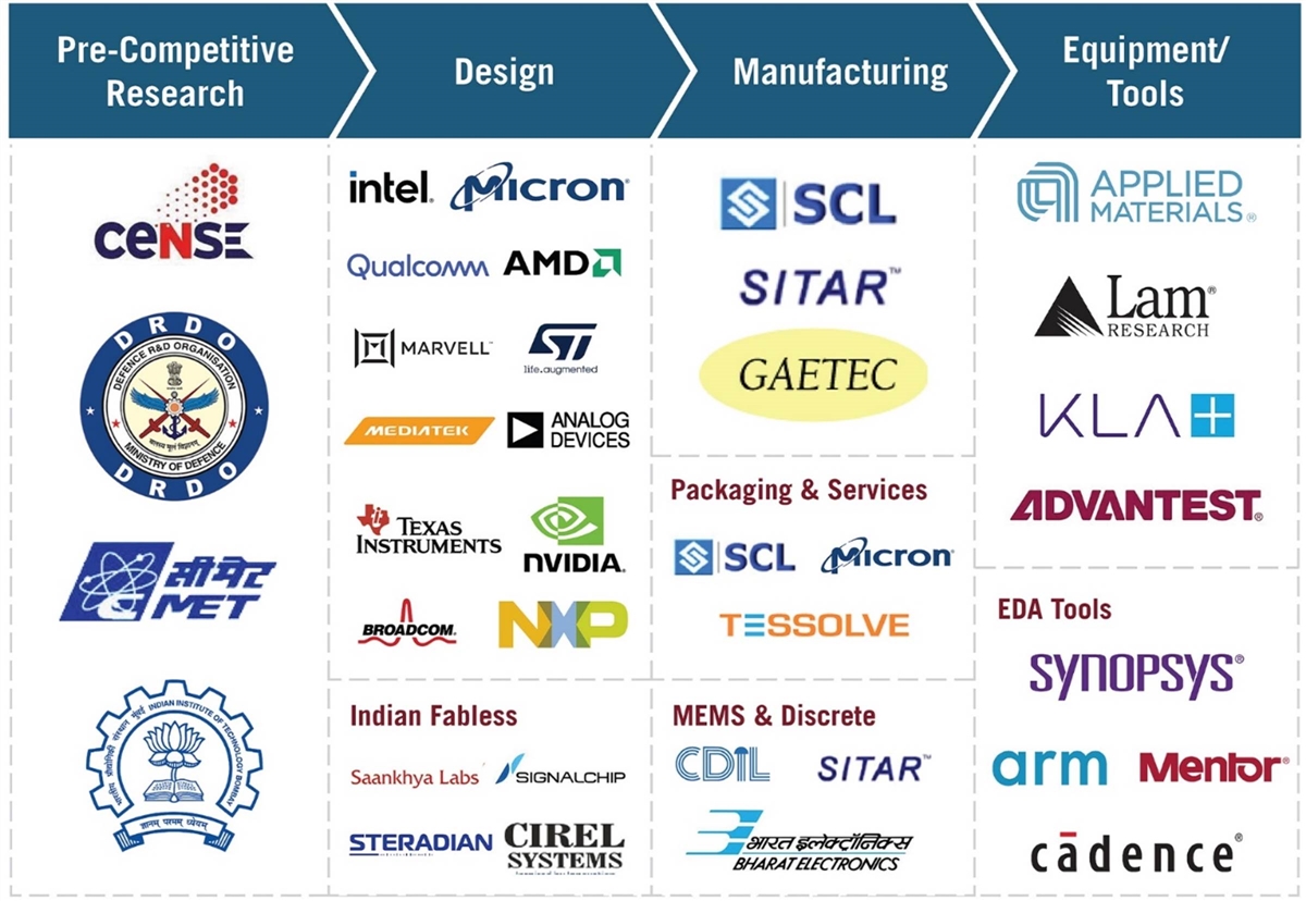
- The Strategic Pivot to Packaging and Design: While high-end leading-edge fabrication remains out of immediate reach, India is aggressively capturing high-value market share in OSAT/ATMP operations and fabless chip design, leveraging its massive pool of VLSI engineering talent.
- Heavyweight Industrial Consortiums: Domestic conglomerates including Tata Group and the Murugapa Group are forging high-stakes joint ventures with international tier-one tech titans such as Taiwan’s Powerchip Semiconductor Manufacturing Corporation (PSMC) and Japan’s Renesas Electronics.
- Structural Bottlenecks Persist: Despite robust capital liquidity and regulatory streamlining, structural challenges including ultra-pure water availability, uninterrupted power grid reliability, and specialized lithography talent acquisition demand vigilant risk management.
The Catalytic Shift: Moving Beyond the Assembly Line
To understand the gravity of India’s current semiconductor trajectory, one must examine the historical policy missteps of the late 20th and early 21st centuries. Previous attempts to jumpstart domestic chip manufacturing foundered on the rocks of bureaucratic friction, inadequate infrastructure scalability, and an absence of downstream electronics manufacturing ecosystems. When the COVID-19 pandemic exposed the fatal vulnerabilities of centralized global supply chains, corporate boardrooms and sovereign treasuries simultaneously woke up to the existential risk of single-point manufacturing failures.
Recognizing that a modern digital economy cannot rely entirely on imported silicon, the Indian administration launched the India Semiconductor Mission (ISM) under the Ministry of Electronics and Information Technology (MeitY). The strategic vision was clear: instead of attempting to immediately rival Taiwan Semiconductor Manufacturing Company (TSMC) at the 2-nanometer or 3-nanometer leading edge, India would build a resilient, vertically integrated foundation anchored in mature nodes, advanced packaging, and world-class chip design.
This pragmatic calibration recognizes that automotive electronics, industrial IoT, consumer appliances, and telecommunications infrastructure rely predominantly on mature and specialty nodes (ranging from 28nm to 180nm). By targeting these segments, India is positioning itself precisely where global demand is structurally sticky and high-volume. Furthermore, cloud compute architecture and artificial intelligence accelerators require sophisticated heterogeneous integration—making advanced packaging facilities a critical choke point that India is now aggressively colonizing.
Key Players and Capital Allocation: Who is Deploying the Billions?
The industrial landscape of India’s semiconductor push is defined by high-conviction bets from both domestic corporate titans and foreign manufacturing legends. Capital allocation strategies vary widely, reflecting a diversified approach to the semiconductor value chain.
The Tata Group’s Foundry and ATMP Gambit
At the vanguard of India’s silicon revolution is the Tata Group. Through Tata Electronics, the conglomerate is spearheading two monumental projects. In Dholera, Gujarat, Tata is partnering with Taiwan’s PSMC to construct a massive semiconductor fabrication facility representing an investment of approximately $11 billion. This fab will focus on mature nodes—specifically 28nm, 45nm, 65nm, and 90nm chips—targeting high-growth verticals in automotive and power management.
Simultaneously, Tata is investing over $3 billion in an advanced OSAT (Outsourced Semiconductor Assembly and Test) facility in Morigaon, Assam. This greenfield project is designed to bridge the crucial post-fabrication gap, handling complex packaging technologies essential for modern processors and memory modules.
The Micron Technology Milestone in Sanand
American memory giant Micron Technology has anchored its faith in India’s regulatory compliance and infrastructure scalability by breaking ground on a $2.75 billion assembly and test facility in Sanand, Gujarat. Micron’s project represents the fastest greenfield semiconductor deployment in recent memory, moving from memorandum of understanding to construction at breakneck speed. This facility focuses on transforming silicon wafers into usable Ball Grid Array (BGA) integrated circuits, directly supplying domestic and global consumer electronics markets.
Other notable players, including CG Power in partnership with Japan’s Renesas Electronics and Thailand’s Stars Microelectronics, are establishing dedicated OSAT units in Sanand, creating a dense geographic cluster that promises significant logistics and talent-sharing efficiencies.
Verified Data and Metrics Breakdown
The following comparative matrix illustrates the scale, technological focus, and capital expenditure of India’s flagship semiconductor projects:
| Company / Joint Venture | Facility Type | Location | Estimated Capex | Primary Technology Node / Focus |
|---|---|---|---|---|
| Tata Electronics & PSMC | Logic Fab | Dholera, Gujarat | ~$11.0 Billion | 28nm, 45nm, 65nm, 90nm Logic & Power ICs |
| Micron Technology | ATMP / OSAT | Sanand, Gujarat | ~$2.75 Billion | DRAM and NAND Flash Packaging & Testing |
| Tata Electronics | ATMP | Morigaon, Assam | ~$3.0 Billion | Advanced Packaging & Flip-Chip Technologies |
| CG Power, Renesas & Stars | OSAT | Sanand, Gujarat | ~$920 Million | Legacy and Power Semiconductors Packaging |
Industry & Market Implications: Winners, Losers, and Economic Ripples
The maturation of India’s semiconductor ecosystem carries profound implications for global supply chain dynamics and domestic macroeconomic indicators.
The Winners: Domestic engineering talent stands out as the ultimate beneficiary. India already produces a significant percentage of the world’s VLSI and chip design verification engineers; domestic fabs create high-paying, intellectually stimulating career pathways that stem brain drain. Furthermore, regional commercial real estate and industrial infrastructure providers in Gujarat, Tamil Nadu, and Karnataka are experiencing unprecedented valuation multiples.
The Losers & Risks: Traditional export-heavy manufacturing hubs in East Asia face incremental competitive pressure as multinational original equipment manufacturers (OEMs) execute dual-sourcing strategies. However, the greater vulnerability lies in execution risk. Semiconductor fabs are exceptionally unforgiving environments. Any failure in water purity, power stability, or chemical supply chain logistics can result in billions of dollars in ruined silicon wafers.
From a macroeconomic perspective, the localization of semiconductor manufacturing promises to dramatically reduce India’s high current account deficit driven by electronics imports, fostering a self-sustaining domestic tech hardware manufacturing loop.
Frequently Asked Questions (People Also Ask)
1. Why is India focusing heavily on mature nodes rather than leading-edge 2nm chips?
While leading-edge chips (under 5nm) command immense media attention, the vast majority of global industrial, automotive, medical, and consumer electronics rely on mature and specialty nodes (28nm to 180nm). By prioritizing mature nodes, India is addressing the highest-volume market segments where global demand is most acute, while building foundational engineering expertise before attempting capital-prohibitive leading-edge nodes.
2. What financial incentives does the Indian government offer semiconductor investors?
Under the Modified Programme for Semiconductors and Display Fab Ecosystem, the central government provides fiscal support of up to 50% of the project cost for semiconductor fabs and display fabs. Additionally, various state governments (such as Gujarat, Karnataka, and Tamil Nadu) offer complementary financial incentives, land subsidies, power tariff concessions, and tax rebates to lower overall capital expenditure.
3. How is India addressing the talent shortage in semiconductor manufacturing?
Recognizing that fabs require specialized chemical, mechanical, and microelectronic engineering talent, the Indian government has partnered with over 100 premier academic institutions (including the Indian Institutes of Technology) to launch specialized VLSI design and semiconductor manufacturing curricula, aiming to train over 85,000 high-tech professionals over the next decade.
4. What role do ATMP and OSAT facilities play in India's semiconductor strategy?
Assembly, Testing, Marking, and Packaging (ATMP) and Outsourced Semiconductor Assembly and Test (OSAT) facilities represent the crucial downstream phase where raw silicon wafers are diced, packaged into usable chips, and rigorously tested. Because ATMP/OSAT projects have slightly faster gestation periods and lower initial capital barriers compared to pure-play fabrication plants, they allow India to immediately integrate into global supply chains while longer-term fabs are being constructed.
Future Outlook: Milestones to Watch
As the calendar moves through 2026 and toward the end of the decade, the narrative surrounding India’s semiconductor industry will shift from groundbreakings and MOU signings to commercial yield rates and volume production. The next crucial milestones include the operationalization of Micron’s Sanand facility, the topping-out of cleanrooms at Tata’s Dholera fab, and the emergence of domestic fabless startup ecosystems supported by government design-linked incentives (DLI).
For global institutional investors, private equity funds, and enterprise tech strategists, ignoring India’s semiconductor transformation is no longer a viable risk-management strategy. The financial architecture is in place, the political will is absolute, and the industrial migration has begun. Silicon sovereignty in South Asia has transitioned from a policy aspiration into an undeniable economic reality.