Executive Takeaways
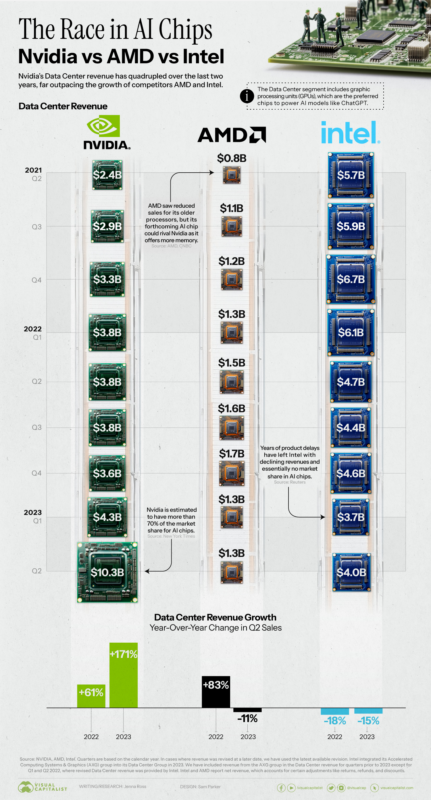
- NVIDIA’s Hardware-Software Flywheel Remains Resilient: Despite intense competitive pressure, NVIDIA maintains an estimated 80% to 88% market share in generative AI acceleration, sustained by its pervasive CUDA ecosystem, proprietary NVLink interconnect fabric, and aggressively compressed product release cadences (Blackwell B200 and Rubin architectures).
- Hyperscaler Custom Silicon Shifts from R&D to Production Scale: Tier-1 cloud service providers (CSPs)—Amazon Web Services, Google Cloud, Microsoft Azure, and Meta—are aggressively scaling in-house Application-Specific Integrated Circuits (ASICs) to lower Total Cost of Ownership (TCO) and mitigate merchant silicon gross margin premiums.
- Advanced Packaging and Memory Supply Form the Real Chokepoint: Market competition is dictated as much by TSMC’s Chip-on-Wafer-on-Substrate (CoWoS) advanced packaging capacity and High-Bandwidth Memory (HBM3e/HBM4) allocations from SK Hynix, Samsung, and Micron as it is by microarchitectural innovation.
- Inference Workloads Open Vector for Disruption: As model development pivots from baseline foundational training to distributed, low-latency enterprise inference, alternative architectures—notably Groq’s Linear Processing Units (LPUs), Cerebras’s wafer-scale engines, and RISC-V startups—are exploiting CUDA’s vulnerabilities.
The Capital Matrix: Why the World’s Balance Sheets Are Flowing to Silicon
Over the trailing twelve months, capital expenditure allocations across Big Tech reached unprecedented velocity, driving global aggregate hyperscale CapEx toward a projected run-rate exceeding $200 billion. At the core of this industrial reallocation is a singular, mission-critical component: parallel compute silicon optimized for tensor mathematics and large matrix operations. Generative artificial intelligence, synthetic media generation, and non-deterministic agentic workflows have upended traditional von Neumann compute paradigms, shifting enterprise infrastructure budgets away from general-purpose CPUs toward massively parallel, high-bandwidth accelerators.
Historically, enterprise data centers allocated less than 15% of compute expenditure directly to graphics processing units (GPUs) and specialized acceleration fabrics. Today, enterprise IT executives and sovereign infrastructure authorities face a paradigm where specialized AI silicon accounts for up to 75% of data center capital deployment. The economic reality is stark: organizations that fail to secure high-density compute capacity face structural degradation in model latency, enterprise automation capabilities, and time-to-market. Consequently, the semiconductor landscape has bifurcated into a high-stakes, multi-front war between incumbent chip designers, trillion-dollar hyperscalers deploying internal ASICs, and venture-backed architecture disruptors attempting to bypass legacy memory constraints entirely.
The Four Factions Reshaping the AI Semiconductor Landscape
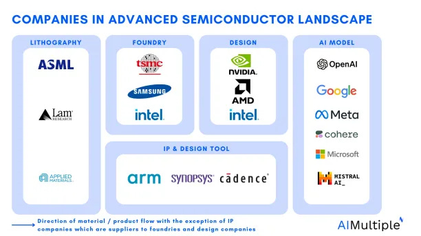
The global AI chipmaking universe spans over thirty institutional players, segmented into four strategic cohorts based on capital structure, microarchitectural trade-offs, and commercial go-to-market models:
1. The Merchant Silicon Titans (General-Purpose AI Accelerators)
This faction represents the standard-bearers of merchant compute silicon—companies whose primary business model is selling discrete accelerator hardware and networking fabrics across diverse OEM and cloud ecosystems:
- NVIDIA: The dominant force, executing a full-stack platform strategy encompassing GPU microarchitectures (Hopper, Blackwell), proprietary interconnects (NVLink, NVSwitch), high-throughput networking (Quantum-X InfiniBand, Spectrum-X Ethernet), and the entrenched CUDA software runtime.
- Advanced Micro Devices (AMD): The primary merchant challenger. AMD’s Instinct MI300X and MI325X platforms utilize an advanced chiplet-based CDNA 3/4 architecture, offering substantial memory capacities that appeal to enterprise operators seeking multi-vendor supply chain redundancy. AMD’s open-source ROCm software stack has narrowed the historical software parity gap through native integration with PyTorch and Triton.
- Intel: Leveraging its Gaudi 3 accelerator platform, Intel targets mid-market enterprise deployments and inference infrastructure, emphasizing performance-per-dollar metrics, native Ethernet networking, and open software abstractions over raw flagship benchmark dominance.
2. The Hyperscaler In-House ASICs (Internal Cloud Workloads)
To reduce reliance on NVIDIA’s 70%+ gross margins and optimize internal inference and training unit economics, the world's largest cloud infrastructure operators have become tier-one fabless semiconductor designers:
- Google (Alphabet): The most operationally mature internal silicon program. Google’s Tensor Processing Units (TPU v5p, TPU v6 "Trillium") power its foundational Gemini models and internal search infrastructure, while being monetized externally via Google Cloud Platform.
- Amazon Web Services (Annapurna Labs): AWS deploys Trainium2 and Inferentia2 chips across its elastic compute fabric, pricing instances at significant discounts to merchant GPU equivalents to preserve ecosystem margins.
- Microsoft: Deploying the Maia 100 accelerator, designed to run foundational Azure OpenAI workloads, alongside the Cobalt 100 CPU, orchestrating an end-to-end bespoke cloud architecture.
- Meta: Operating the Meta Training and Inference Accelerator (MTIA v1/v2), optimized specifically for recommendation algorithms, ad rank modeling, and internal Llama infrastructure workloads.
- Apple: Utilizing custom Silicon (M-series and A-series Neural Engine/NPU fabrics) to power on-device Apple Intelligence, alongside data-center-level deployment of proprietary Apple-silicon server clusters.
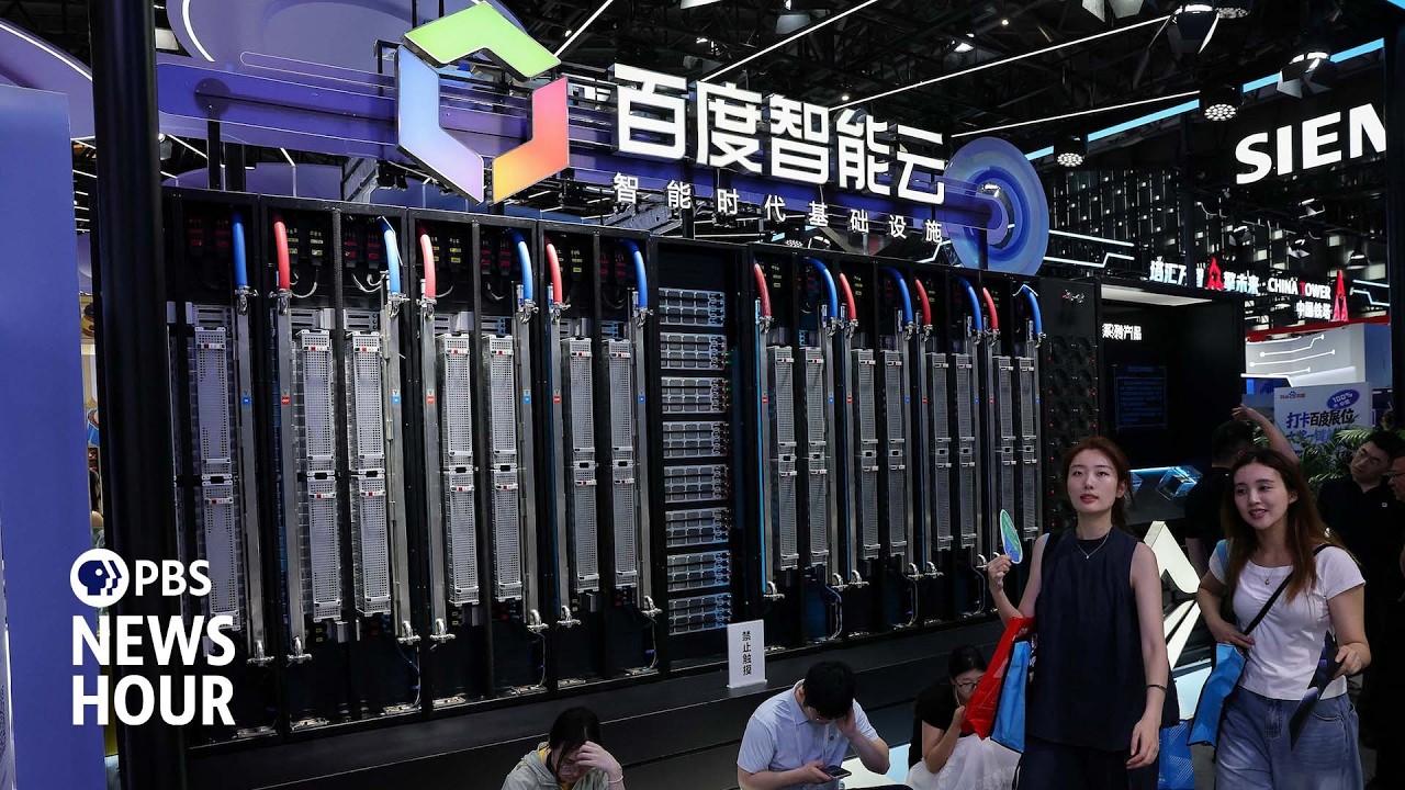
- Alibaba Cloud & Baidu: Deploying the Hanguang 800 and Kunlunxin AI accelerators respectively, insulating Chinese digital platforms from international hardware supply chain fluctuations.
3. Venture-Backed Disruptors and Architectural Radicals
Unencumbered by legacy silicon designs or backwards-compatibility constraints, specialized startups are engineering compute engines designed expressly for transformer and mixture-of-experts (MoE) workloads:
- Groq: Pioneered the Language Processing Unit (LPU), an architecture engineered around high-speed Static Random-Access Memory (SRAM) instead of High-Bandwidth Memory (HBM). By eliminating external memory lookups, Groq achieves unprecedented token-generation velocity for low-latency inference workloads.
- Cerebras Systems: Champion of the Wafer-Scale Engine (WSE-3), a single, dinner-plate-sized silicon wafer comprising 4 trillion transistors and 900,000 AI-optimized cores, bypassing inter-chip networking latency entirely by housing an entire cluster on a single physical substrate.
- Tenstorrent: Led by industry pioneer Jim Keller, Tenstorrent leverages open-standard RISC-V architectures and cost-effective chiplet designs to build modular, customizable AI engines with an emphasis on developer ownership and architectural transparency.
- SambaNova Systems: Features the SN40L Reconfigurable Dataflow Unit (RDU), orchestrating algorithmic dataflows natively in hardware rather than executing rigid instruction sets, maximizing parameter capacity for massive enterprise models.
- Etched: Developing "Sohu," an ASIC intentionally hardwired to execute transformer attention mechanisms exclusively, claiming exponential cost-to-performance advantages over general-purpose matrix compute engines.
- d-Matrix, Untether AI, and Axelera AI: Innovating in Digital In-Memory Computing (DIMC) and edge acceleration, physically co-locating mathematical operations inside memory arrays to slash thermal dissipation and memory-transfer latency.
4. Sovereign Compute and Embedded Edge Silicon
National security directives and the dispersion of AI into endpoint hardware have generated a robust ecosystem of specialized silicon providers:
- Qualcomm: Dominating high-performance edge inference across mobile and automotive tiers with its Hexagon NPU, alongside enterprise offerings via its Cloud AI 100 platform.
- Huawei: Powering China's sovereign AI infrastructure through the Ascend 910B and 910C processors, integrated with the CANN software architecture to build end-to-end indigenous high-performance computing clusters.
- Biren Technology, Moore Threads, and Enflame: Chinese fabless designers developing high-compute alternatives to Western merchant GPUs under domestic self-reliance initiatives.
- NXP, STMicroelectronics, and Texas Instruments: Driving low-power, deterministic microcontrollers integrated with specialized machine learning blocks for industrial automation, robotics, and edge telematics.
Silicon Architecture & Performance Benchmark Comparison
The operational metrics governing AI silicon evaluation have moved beyond raw theoretical TFLOPS. Institutional buyers evaluate accelerators across total memory bandwidth, interconnect scaling, thermal design power (TDP), and deployment topologies:
| Platform / Accelerator | Primary Architecture | Memory Spec & Bandwidth | Interconnect Fabric | Peak Compute (FP8/BF16) | Primary Deployment Profile |
|---|---|---|---|---|---|
| NVIDIA B200 (Blackwell) | Dual-Die GPU (TSMC 4NP) | 192GB HBM3e 8.0 TB/s |
NVLink 5 (1,800 GB/s bidirectional) |
~4.5 PFLOPS FP8 | Hyperscale LLM Training & Enterprise MoE Inference |
| AMD Instinct MI300X | Modular Chiplet CDNA 3 | 192GB HBM3 5.3 TB/s |
Infinity Fabric (896 GB/s bidirectional) |
~2.6 PFLOPS FP8 | Large-Context Inference & Open-Source Foundational Training |
| Google TPU v5p | Bespoke Cloud ASIC | 95GB HBM2e 2.76 TB/s |
Inter-Core Optical Circuit Switching (OCS) | ~459 TFLOPS BF16 | Internal Alphabet Services & Sovereign GCP Pods |
| AWS Trainium2 | Internal Fabless ASIC | Up to 96GB HBM Scalable Tier |
NeuronLink-v2 Fabric | ~4x Compute vs Trainium1 | Elastic AWS Infrastructure & Low-Cost Fine-Tuning |
| Groq LPU | Tensor Streaming Processor | 230MB On-Chip SRAM 80 TB/s |
Direct Chip-to-Chip Proprietary Mesh | ~750 TFLOPS FP8 | Ultra-Low-Latency Real-Time LLM Token Generation |
| Cerebras WSE-3 | Wafer-Scale Monolithic | 44GB On-Die SRAM 21 PB/s |
Switched Fabric on Silicon Substrate | ~125 PFLOPS FP16/Sparse | Massive AI Training Supercomputing Centers |
Supply Chain Bottlenecks: CoWoS Packaging, HBM, and Fab Consolidation
While algorithmic efficiency captures headlines, enterprise silicon delivery is governed by a concentrated manufacturing bottleneck. The decisive gating factor for AI accelerator availability is not front-end wafer fabrication at 3-nanometer or 5-nanometer process nodes; rather, it is back-end advanced packaging and the physical integration of dynamic memory.
Taiwan Semiconductor Manufacturing Company (TSMC) maintains a near-monopoly on high-performance packaging through its proprietary Chip-on-Wafer-on-Substrate (CoWoS) technology. CoWoS enables the dense, multi-die integration of compute silicon with HBM stacks on a passive silicon interposer. With NVIDIA, AMD, Broadcom (for Google ASICs), and Amazon consuming TSMC's packaging allocation, lead times for advanced compute clusters have historically stretched past 40 weeks.
Concurrently, the integration of High-Bandwidth Memory (HBM3e and next-generation HBM4) has introduced a volatile component into merchant silicon bills of materials (BOM). SK Hynix, Samsung Electronics, and Micron Technology face technical yield hurdles in thermal compression non-conductive film (TC-NCF) bonding and advanced Through-Silicon Via (TSV) manufacturing. This supply constraint grants NVIDIA asymmetric pricing leverage, allowing it to preserve industry-leading margins while downstream enterprise clients face elevated infrastructure cost burdens.
Software Ecosystems: The Real Moat Against Architectural Parity
Hardware specifications alone do not determine commercial victory. The enduring defensive barrier protecting NVIDIA’s merchant primacy is its software ecosystem: CUDA (Compute Unified Device Architecture). Over an eighteen-year horizon, CUDA has integrated into global computational science, engineering, and artificial intelligence curricula. The vast majority of low-level optimization kernels, precision libraries (cuDNN, TensorRT), and algorithmic implementations were compiled natively for NVIDIA microarchitectures.
Competitors have historically stumbled by shipping competitive silicon alongside incomplete, fragmented software layers. However, this defensive moat faces structural shifts through two mechanisms:
- High-Level Compiler Abstractions: The ascent of PyTorch 2.0, OpenAI’s Triton language, and vLLM inference engines allows developers to write optimized kernels without manual CUDA programming. These frameworks decouple the underlying hardware target from high-level model definitions, lowering the switching cost to alternative silicon.
- Open Ecosystem Standards: AMD’s investments into ROCm, Intel’s unified oneAPI initiative, and cross-industry consortiums (like the Ultra Ethernet Consortium designed to dismantle NVIDIA’s proprietary InfiniBand hold) are democratizing cluster deployment and reducing vendor lock-in.
Frequently Asked Questions (People Also Ask)
Why can't competing chipmakers easily replicate NVIDIA’s AI performance?
Replicating NVIDIA’s capability requires solving three interdependent engineering challenges simultaneously: compute microarchitecture, multi-node networking fabrics, and low-level software integration. While rivals can produce silicon dies with equivalent mathematical compute density, NVIDIA excels at multi-GPU clustering through its proprietary NVLink interconnect and InfiniBand networking platforms. Furthermore, the global software developer base is fundamentally native to CUDA, meaning non-NVIDIA silicon requires substantial code translation, compiler refactoring, and stability optimization before production readiness.
What is the difference between an AI GPU and a custom AI ASIC?
An AI GPU (Graphics Processing Unit) is a flexible, highly parallel processor designed to handle a broad spectrum of matrix mathematical workloads, making it capable of running different model architectures, scientific simulations, and graphic pipelines. An AI ASIC (Application-Specific Integrated Circuit), such as Google’s TPU or Groq’s LPU, is physically hardwired to optimize a narrower, precise set of operations—specifically tensor contractions or transformer attention. ASICs sacrifice architectural versatility in exchange for superior power efficiency, lower cost-per-inference token, and dedicated performance for specific model topologies.
How does High-Bandwidth Memory (HBM) impact total enterprise AI infrastructure cost?
High-Bandwidth Memory (HBM) stacks dynamic memory dies vertically using Through-Silicon Vias (TSVs), placing them on the same package as the accelerator processor. This architecture provides data transfer rates exceeding several terabytes per second, which prevents compute cores from stalling during memory-bound Large Language Model operations. However, HBM manufacturing yields are structurally lower than standard DDR5 memory, significantly increasing component BOM costs. For enterprise buyers, this dynamic inflates accelerator pricing, making memory capacity and memory bandwidth the primary cost drivers in modern data center capital allocations.
Will custom hyperscaler chips (AWS Trainium, Google TPU) eliminate merchant chipmakers?
Custom hyperscaler ASICs are not intended to eliminate merchant chipmakers entirely; rather, they serve as a strategic cost-containment and margin-preservation hedge. Hyperscalers design internal silicon to power their own native applications (such as AWS Bedrock, Google Search, and Meta’s recommendation engines) and provide cost-effective tiers for enterprise cloud tenants. However, merchant accelerators from NVIDIA and AMD will retain dominant demand among Fortune 500 enterprises, on-premises private cloud operators, and sovereign AI entities that require general-purpose hardware portability and independent infrastructure autonomy.
The Strategic Horizon: The Post-CoWoS Era and Enterprise Implications
The enterprise AI chip ecosystem is entering an inflection point characterized by workload maturation. As foundation model training yields to enterprise inference deployments, compute demand will shift from raw multi-node scaling toward latency-per-token, energy efficiency, and operational TCO. Silicon solutions that prioritize energy-efficient inference—such as dynamic in-memory computing architectures, analog acceleration, and compact ASICs deployed at the edge—will secure an expanding share of enterprise compute budgets.
For institutional capital allocators, CIOs, and data center operators, the coming 24 to 36 months will require continuous portfolio risk mitigation. Reliance on a single merchant silicon vendor exposes organizations to persistent capital expenditure inflation and supply chain concentration risks. The emerging consensus across enterprise technology leadership is clear: the future of artificial intelligence infrastructure will not belong to a single monolithic platform, but to a diversified, heterogenous computing environment that spans merchant GPUs, hyperscaler ASICs, and specialized architectural accelerators.