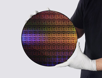
NEW YORK & BENGALURU — In a move that redraws the geopolitical and technological map of the global semiconductor industry, IBM has shattered the theoretical physical limits of silicon. On June 25, 2026, the technology giant officially debuted the world’s first sub-1 nanometer (sub-1nm) chip technology, a milestone once deemed commercially impossible by many of the world's leading physicists and material scientists.
Built on a radical, proprietary "nanostack" 3D chip architecture, IBM's newest breakthrough packs an astonishing 100 billion transistors onto a single sliver of silicon no larger than a human fingernail. The development arrives at a critical juncture for the global tech economy, which is currently buckling under the immense, unsustainable power demands of generative artificial intelligence and hyperscale data centers.
By bypassing the architectural limits of traditional planar and gate-all-around (GAA) nanosheet structures, IBM's sub-1nm technology promises to unlock unprecedented computational density while slashing energy consumption. Industry analysts are already calling it the most significant leap in semiconductor fabrication since the invention of the integrated circuit.
Inside the "Nanostack": How IBM Defied Physics
For the past decade, the semiconductor industry has wrestled with the looming threat of "quantum tunneling"—a physical phenomenon where electrons jump across barriers when transistor gates become too small, leading to current leakage, overheating, and systemic chip failure. To push past the 2-nanometer barrier, IBM’s research division at the Albany NanoTech Complex in New York abandoned conventional vertical stacking models in favor of a revolutionary "nanostack" 3D architecture.
The "nanostack" technique allows engineers to stack active transistor channels vertically in highly dense, multi-layer 3D arrays, utilizing advanced cobalt and ruthenium metallization processes instead of traditional copper. This minimizes resistance, dramatically reduces heat dissipation, and allows for precise electron control at the atomic scale.
Key Architectural Innovations of IBM’s Sub-1nm Node:
- 3D Nanostack Integration: Vertically arrays multiple nanosheet layers on a single die, effectively tripling transistor density without expanding the horizontal footprint.
- Atomic Layer Deposition (ALD): Employs next-generation extreme ultraviolet (EUV) lithography to manipulate materials at the single-atom layer, ensuring structural integrity below 10 angstroms.
- Backside Power Delivery: Decouples the power network from the signal-carrying metal lines, placing it on the underside of the wafer to eradicate voltage drops and boost thermal efficiency.
The AI Catalyst: Slashing Data Center Power Demands

The primary commercial driver for this technology is the insatiable, energy-hungry nature of modern artificial intelligence. Today’s AI clusters, powered by massive arrays of 3nm and 4nm GPUs, are pushing local power grids to their absolute limits. IBM’s sub-1nm architecture offers a monumental paradigm shift.
According to IBM’s technical brief, when compared to the current industry-standard 3nm chips found in top-tier consumer electronics and AI servers, the sub-1nm nanostack chip is projected to deliver either a 75% reduction in power consumption at the same performance level, or a 50% increase in computational performance within the same power envelope.
For hyperscalers like Microsoft, Amazon Web Services, and Google, migrating to sub-1nm architecture could mean billions of dollars saved in electricity and cooling infrastructure, significantly lowering the carbon footprint of global AI models.
Comparing the Generations: The Leap to Sub-1nm
To understand the scale of IBM's achievement, it is helpful to look at how this technology stacks up against previous manufacturing nodes:
| Metric / Node | 5nm Node (2020) | 3nm Node (Current Standard) | IBM Sub-1nm Nanostack (2026) |
|---|---|---|---|
| Transistor Count (Fingernail Size) | ~30 Billion | ~50 Billion | ~100 Billion |
| Power Reduction (vs. 5nm Baseline) | Baseline | ~35% Savings | ~85% Savings |
| Performance Increase (vs. 5nm Baseline) | Baseline | ~20% Boost | ~70% Boost |
| Primary Architecture Style | FinFET (2D) | GAA Nanosheet (2.5D) | Nanostack 3D (Atomic-Scale) |
Geopolitical Implications and the Race to Commercialization
IBM's announcement has sent shockwaves through global capital markets and the halls of government. Under the framework of the U.S. CHIPS and Science Act, the race to secure domestic leading-edge manufacturing capabilities has become a matter of national security. While IBM is a fabless design pioneer—relying on manufacturing partners like Samsung and potentially Intel Foundry Services to bring its designs to high-volume production—this breakthrough gives the Western semiconductor alliance immense leverage.
"We are looking at a fundamental shift in the global balance of computational power," says an executive-level source close to the U.S. Department of Commerce. "The nation or alliance that successfully commercializes sub-1nm technology first will hold the keys to the future of military AI, cryptography, and quantum-resistant computing."
While mass commercial production of IBM's sub-1nm technology is not expected until the late 2020s, the intellectual property foundation laid today positions IBM as the ultimate gatekeeper of next-generation computing hardware.
Frequently Asked Questions (FAQ)
When will consumer devices and AI data centers see sub-1nm chips in the market?
While the architectural technology is now proven in laboratory environments, high-volume manufacturing (HVM) is highly complex. Industry insiders estimate that commercial implementation—likely starting with specialized AI accelerators and enterprise cloud servers—will begin pilot production by late 2028, with consumer smartphones and PCs adopting the technology around 2029 or 2030.
How does "nanostack" 3D technology solve the problem of quantum tunneling?
In traditional flat structures, as transistors get smaller, the barriers between gates become too thin, allowing electrons to slip through uncontrollably. IBM's 3D Nanostack solves this by vertically orienting the channels and utilizing new, ultra-dense atomic-layer materials like cobalt and ruthenium. This geometry provides superior electrostatic control, keeping the "gates" tightly sealed and stopping unwanted electron leakage in its tracks.