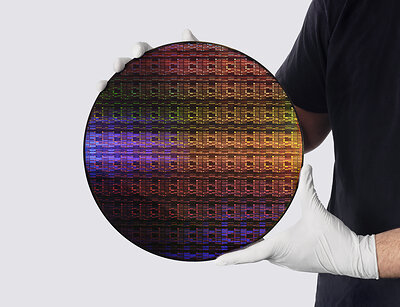
NEW YORK — In a monumental breakthrough that redefines the outer boundaries of modern physics and computing, International Business Machines (IBM) has officially debuted the world’s first sub-1 nanometer semiconductor technology. Announced late last week, the landmark engineering feat introduces an entirely new architectural paradigm designed to bypass the decades-old physical roadblocks threatening Moore's Law.
The announcement, sourced directly from the IBM Newsroom and verified across global technology markets, centers on a revolutionary "nanostack" 3D chip architecture. According to lead engineers, this cutting-edge design successfully crams nearly 100 billion microscopic transistors onto a sliver of silicon no larger than a human fingernail. The commercial implications for enterprise data centers, generative artificial intelligence infrastructure, and consumer electronics are expected to send seismic shockwaves through the global tech supply chain.
The Engineering Marvel: Inside the 'Nanostack' Breakthrough
For years, semiconductor manufacturers have grappled with quantum tunneling—a phenomenon where electrons leak through microscopic barriers as transistors shrink below the 2-nanometer threshold, causing severe electrical short circuits and catastrophic heat generation. IBM’s research and development division has circumvented this fundamental obstacle by moving away from traditional planar scaling.
Instead, the newly unveiled sub-1 nm technology leverages a proprietary vertical "nanostack" 3D integration technique. By routing electrical pathways upward in multi-layered tiers rather than crowding them horizontally across a flat surface, IBM has effectively maximized spatial density without compromising electron mobility or thermal stability.
- Transistor Density: Nearly 100 billion active components packed onto a single fingernail-sized footprint.
- Architectural Shift: Vertical 3D "nanostack" design replaces conventional 2D planar scaling.
- Thermal Management: Advanced material integration prevents the overheating typically associated with extreme sub-nanometer densities.
- Power Efficiency: Delivers massive reductions in energy consumption, directly addressing the global data center power crunch.
Unlocking Infinite Scale for Generative AI Applications

The timing of IBM’s breakthrough could not be more critical. As hyperscalers and enterprise tech giants spend tens of billions of dollars constructing massive data centers to train increasingly complex large language models (LLMs), the primary bottleneck has shifted from software algorithms to sheer electrical power availability and chip cooling capacity.
Industry analysts point out that IBM’s sub-1 nm chip architecture could unlock massive power savings across the entire AI ecosystem. By drastically lowering the power-per-watt ratio required to execute heavy matrix multiplications and neural network inferences, the new technology promises to slash operational overhead for cloud providers while enabling edge-AI devices—such as smartphones and autonomous vehicles—to run supercomputer-grade intelligence locally.
| Metric / Feature | Previous Industry Standard (2nm) | IBM Sub-1 Nanometer Technology |
|---|---|---|
| Node Size | 2 Nanometers | Sub-1 Nanometer (<1nm) |
| Transistor Count | ~50 Billion per chip | Nearly 100 Billion per chip |
| Architecture | GAA (Gate-All-Around) 2D | 3D "Nanostack" Vertical Integration |
| Primary Benefit | Incremental density gains | Massive AI power savings & thermal control |
Market Impact and the Global Semiconductor Race
The unveiling places IBM once again at the bleeding edge of materials science and microelectronics. While rivals like TSMC, Samsung, and Intel have made aggressive strides toward commercializing 2nm and 1.4nm nodes over the next few years, IBM’s leap directly into sub-1 nanometer territory alters competitive timelines across the globe.
Financial markets reacted swiftly to the news, with technology indices noting heightened investor interest in advanced packaging equipment makers, lithography suppliers, and specialized substrate manufacturers. The ability to manufacture chips at this scale requires equally advanced extreme ultraviolet (EUV) lithography and precision etching tools, setting off a fresh wave of capital expenditure expectations across the supply chain.
Future Outlook and Commercialization Roadmap
Moving from a laboratory breakthrough to mass-market foundry production remains a notoriously complex hurdle in the semiconductor industry. IBM has historically utilized a licensing and joint-development model for its semiconductor innovations, partnering with global fabrication giants to bring research bench discoveries into commercial fabrication plants.
As enterprise adoption of artificial intelligence continues its exponential trajectory, the demand for silicon capable of handling heavier compute loads without melting data center grids will dictate corporate winners and losers. With the introduction of its sub-1 nm nanostack architecture, IBM has laid down a definitive marker, proving that the physical limits of silicon can still be pushed far beyond conventional imagination.
Frequently Asked Questions
What makes IBM's new sub-1 nm chip different from existing processors?
Unlike traditional 2D chips that crowd transistors horizontally, IBM utilizes a revolutionary 3D "nanostack" architecture. This vertical stacking allows nearly 100 billion transistors to fit onto a fingernail-sized chip while overcoming quantum tunneling and thermal bottlenecks.
How does this technology impact artificial intelligence applications?
The sub-1 nm architecture delivers massive power savings and enhanced energy efficiency. This directly addresses the massive power consumption challenges faced by modern AI data centers, enabling faster model training and execution with significantly lower electrical overhead.



:max_bytes(150000):strip_icc()/GettyImages-2295150353-20570f3ab41c46c2a6a7c08cf9a9786c.jpg)