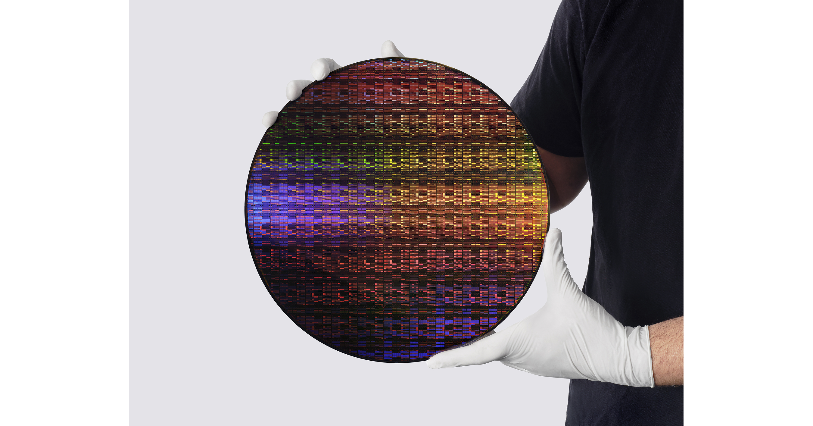
NEW YORK — In what industry veterans are calling a watershed moment for modern computing, IBM has officially pulled back the curtain on the world’s first sub-1 nanometer chip technology. Announced today via the IBM Newsroom, the breakthrough shatters historical scaling roadblocks that have vexed semiconductor physicists for over a decade. By defying conventional physical constraints, IBM is poised to rewrite the rules of enterprise computing, mobile architecture, and heavy-duty artificial intelligence.
The announcement arrives at a pivotal juncture. As the generative AI boom demands ever-expanding compute power while simultaneously exposing a brutal ceiling in global energy grids, hardware efficiency has become the holy grail of tech. IBM’s radical new architecture directly answers this crisis, promising a generational leap in performance-per-watt that could alleviate looming power shortages across hyper-scale data centers.
Engineering the Impossible: Inside the 'Nanostack' 3D Architecture
At the heart of IBM’s breakthrough is a revolutionary design paradigm dubbed “nanostack” 3D chip architecture. Traditional semiconductor scaling relied heavily on shrinking transistors horizontally across a 2D plane—a methodology that is rapidly approaching the absolute quantum limits of silicon, where electrons begin to leak unpredictably through microscopic barriers.
Instead of hitting a dead end, IBM’s research and development teams went vertical. The newly unveiled sub-1nm technology packs nearly 100 billion transistors onto a single piece of silicon no larger than a human fingernail. By stacking active semiconductor layers in a three-dimensional matrix, the nanostack architecture allows signals to travel shorter distances, drastically reducing latency while slashing thermal output.
- Unprecedented Density: Nearly 100 billion functional transistors housed on a fingernail-sized die.
- Quantum-Resistant Design: Novel gate-all-around (GAA) material integrations mitigate electron leakage at sub-atomic scales.
- Thermal Efficiency: Vertical heat dissipation channels prevent the extreme thermal throttling common in legacy dense processors.
Unlocking Massive Power Savings for the AI Era

The immediate commercial beneficiary of IBM’s sub-1nm breakthrough will undoubtedly be the artificial intelligence sector. Current large language models (LLMs) and multi-modal generative networks require sprawling, power-hungry server farms that consume electricity on the scale of small cities. Utility companies have repeatedly warned that the data center expansion required for general-purpose AI is outstripping grid capacities.
According to preliminary architectural telemetry released by IBM, the new sub-1nm processors unlock massive power savings—potentially cutting inference and training energy overhead by up to 50 compared to current 2nm and 3nm nodes currently rolling out across the market. This drastic reduction means hyperscalers can train heavier, more complex models with a fraction of the carbon footprint and electricity cost.
"IBM’s latest chip breakthrough marks a landmark moment in microelectronics," noted senior engineering leads at the company during the global press briefing. "We are no longer just pushing silicon to its limits; we are establishing an entirely new physics framework for the next fifty years of computing."
At a Glance: The Sub-1nm Architecture vs. Current Tech
| Metric | Current Industry Standard (3nm/2nm) | IBM Sub-1nm Technology |
|---|---|---|
| Transistor Count | ~30 to 50 Billion per die | ~100 Billion per fingernail-sized die |
| Architecture | Primarily 2D/FinFET/Early GAA | Revolutionary "Nanostack" 3D Architecture |
| Primary Target | General mobile & cloud computing | High-density AI workloads & enterprise servers |
| Energy Efficiency | Baseline standard | Massive power savings (up to 50% reduction in key workloads) |
Market Implications and the Road Ahead
Wall Street and global semiconductor supply chains are already reacting to the news. The race to sub-1nm was widely expected to take the industry well into the 2030s, making IBM’s premature victory a disruptive shock to competitors like TSMC, Intel, and Samsung. While commercial mass production timelines have not yet been fully detailed, enterprise partners are expected to receive initial evaluation samples for data center integration within the next year.
For investors, the development signals that hardware obsolescence cycles are accelerating rather than slowing down. Companies that fail to adapt to sub-1nm and 3D-stacked paradigms risk seeing their AI infrastructure rendered obsolete overnight as power constraints tighten regulatory and financial scrutiny.
Frequently Asked Questions
What makes IBM's new chip "sub-1 nanometer"?
The term refers to the scale of the critical feature dimensions within the chip's architecture. By dropping below the 1-nanometer threshold, IBM has manipulated matter at the atomic level, utilizing advanced vertical 3D stacking ("nanostack") to bypass the physical limitations that stop traditional 2D chips from scaling further.
When will these chips be available commercially?
While IBM has debuted the working technology and proven its feasibility, commercial scaling and foundry integration take time. Enterprise evaluation samples are anticipated within the near future, with broader commercial data center deployment expected as manufacturing yields mature over the next few years.