Executive Takeaways
- The Trillion-Dollar Acceleration: Global semiconductor revenues are tracking to eclipse the historic $1 trillion milestone ahead of prior consensus estimates, catalyzed by an unrelenting $380 billion hyperscaler capital expenditure cycle dedicated to generative and agentic AI clusters.
- The Sub-2nm and Backside Power Convergence: Commercialization of 2nm-class nodes (TSMC N2, Intel 18A, Samsung SF2) integrating Gate-All-Around (GAA) nanosheets and Backside Power Delivery Networks (BSPDN) is structurally breaking the classical Dennard scaling ceiling to unlock up to 30% power-performance-area gains.
- Interconnects Surpass Raw Compute: Advanced packaging, High-Bandwidth Memory (HBM4) running on native 2048-bit base dies, and the commercial ramp of Co-Packaged Optics (CPO) have shifted capital allocation priorities from monolithic processor speed to interconnect density and micro-joule-per-bit transit efficiency.
- Structural Disruption in Merchant Silicon: Custom hyperscaler Application-Specific Integrated Circuits (ASICs) and domain-specific accelerators are capturing upwards of 28% of tier-1 cloud compute footprints, compressing valuation multiples for legacy general-purpose hardware suppliers.
The global semiconductor industry has crossed a geopolitical and technological Rubicon. Heading into 2026, the sector is no longer tethered to traditional consumer hardware refresh cycles or PC volume volatility. Instead, it operates as the foundational capital asset of the global economy, driven by an enterprise artificial intelligence infrastructure race characterized by non-linear computational demands and sovereign industrial policies.
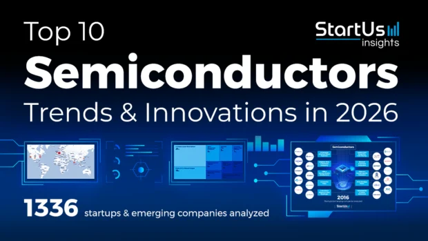
According to analysis synthesized from primary wire data via StartUs Insights and industry supply chain channel checks, semiconductor architecture in 2026 is undergoing its most aggressive architectural reconfiguration in four decades. The historical pursuit of single-die Moore’s Law scaling has yielded to a multi-dimensional matrix of heterogeneous packaging, optical interconnect integration, wafer-level power management, and sovereign supply chain bifurcation. For institutional allocators, foundry strategists, and enterprise technology officers, deciphering these technical pivots is paramount to evaluating capital allocation, enterprise ROI, and competitive moats.
The 10 Architectural and Structural Trends Dominating 2026

1. Commercial Sub-2nm Nodes and GAA Nanosheet Maturation
The transition from FinFET to Gate-All-Around (GAA) architectures has reached commercial maturity at the sub-2nm frontier. TSMC’s N2, Intel’s 18A/14A pipeline, and Samsung’s SF2 processes are executing high-volume tape-outs for enterprise accelerators. GAA nanosheet channels provide electrostatic control that eradicates the sub-threshold leakage plaguing leading-edge nodes, allowing drive currents to scale under ultra-low operational voltages. This transition demands High-Numerical Aperture (High-NA) 0.55 NA Extreme Ultraviolet (EUV) lithography systems, fundamentally shifting tool economics as single scanners exceed $380 million, consolidating the leading-edge foundry landscape into an ultra-exclusive oligopoly.
2. Backside Power Delivery Networks (BSPDN)
Signal and power line congestion on the front side of the silicon die historically degraded clock speeds via resistive parasitic drops (IR drop). In 2026, Intel’s PowerVia and TSMC’s Super Power Rail decouple power routing entirely, moving thick, low-resistance metal power rails to the reverse side of the thinned wafer. By isolating the interconnect stack to signal integrity alone, BSPDN yields a 10% to 15% frequency increase, up to a 20% area recovery, and an essential mitigation vector for thermal hot spots in megawatt-scale data center environments.
3. HBM4 and the 2048-Bit Memory Interface Leap
The memory wall has served as the single greatest governor on large multimodal model (LMM) inference and training efficiency. The 2026 production ramp of HBM4 shatters legacy memory topologies. Transitioning from the conventional 1024-bit interface to a 2048-bit ultra-wide bus routed on advanced 4nm/3nm base logic dies, HBM4 achieves over 2.5 to 3.0 terabytes per second (TB/s) of bandwidth per stack. Because the base die is fabricated on leading-edge CMOS logic rather than standard DRAM processes, foundries and memory titans (SK Hynix, Micron, Samsung) have forged historic structural co-design alliances, rearranging traditional gross-margin distributions.
4. Co-Packaged Optics (CPO) and Silicon Photonics Penetration
Electrical signal attenuation over copper traces at 224 Gbps and emerging 448 Gbps SerDes architectures has hit thermal and physical barriers. In 2026, Co-Packaged Optics moves photonics from external transceivers directly onto the multi-chip substrate, colocating optical engines alongside the central compute silicon. By transforming electrons into photons millimeters from the arithmetic logic units, data centers are driving optical transit power consumption down from 15–20 picojoules per bit (pJ/bit) to sub-4 pJ/bit, unlocking massive power savings for hyperscale switch fabrics.
5. The UCIe 2.0 Standard and Heterogeneous Chiplet Ecosystems
Monolithic dies designed at the reticle limit are economically unsustainable for complex multi-core AI accelerators. The universalization of the Universal Chiplet Interconnect Express (UCIe 2.0) standard has formalized an interoperable marketplace for modular silicon. Disaggregated architectures decouple analog I/O, SRAM cache tiles, and leading-edge logic compute cores across optimized disparate process nodes (e.g., 16nm for analog I/O, 2nm for logic cores), substantially improving gross yield economics and driving down design cycles for bespoke enterprise silicon.
6. The Hyperscaler Custom ASIC Tipping Point
Merchant GPU architectures, while versatile, carry a substantial architectural overhead for strictly defined inference workloads. In 2026, custom Cloud ASICs (spearheaded by platforms like Google TPU v6, AWS Trainium3/Inferentia, and Microsoft Maia) represent nearly a third of all cloud infrastructure deployments. Hyperscalers are accepting high upfront non-recurring engineering (NRE) costs to circumvent merchant silicon gross margins, capturing enterprise ROI through micro-tailored precision formats (FP4, MXFP6) optimized for specific algorithmic footprints.
7. Wide-Bandgap Materials: GaN and SiC Inside the Megawatt Server
The power delivery challenge is no longer confined to the nanometer level; it now threatens the grid. Power distribution units (PDUs) and server-rack voltage regulators are rapidly transitioning from legacy silicon MOSFETs to Gallium Nitride (GaN) and Silicon Carbide (SiC) semiconductors. These wide-bandgap materials manage significantly higher breakdown fields, switching frequencies, and operational temperatures. As server racks demand 100 kW to 150 kW per enclosure, GaN-on-Silicon power stages reduce thermal loss by up to 40%, ensuring compliance with strict global environmental regulations and grid constraints.
8. AI-Autonomous Electronic Design Automation (EDA 2.0)
Chip complexity has exceeded human manual placement and physical design verification capacities. In 2026, algorithmic, agentic AI frameworks within EDA tool suites (Synopsys, Cadence, Siemens EDA) run autonomous floorplanning, macro placement, and clock-tree synthesis. Generative EDA tools reduce complex leading-edge tape-out timelines from 18 months to under six months, optimizing power-performance-area (PPA) parameters while mitigating the chronic global shortage of skilled VLSI engineering talent.
9. Neuromorphic and In-Memory Edge Compute
The computational bottleneck of running edge AI is governed by the energy expended moving weights from memory to arithmetic registers (the von Neumann bottleneck). In-Memory Computing (IMC) using resistive RAM (ReRAM), phase-change memory (PCM), and specialized neuromorphic analog arrays execute vector-matrix multiplication directly inside the memory cell. This trend is unlocking true ambient intelligence in 2026: real-time computer vision, acoustic event detection, and autonomous drone navigation operating under fractional-watt power budgets without continuous cloud connectivity.
10. Sovereign Supply Chains and Fab Regionalization
The geopolitical concentration of advanced packaging and fabrication in the Taiwan Strait remains the semiconductor industry’s most acute systemic vulnerability. By 2026, multi-billion-dollar state incentives from the U.S. CHIPS and Science Act, the EU Chips Act, and Japanese subsidies have yielded operational, leading-edge capacity across Arizona, Ohio, Dresden, and Kumamoto. While operational costs in these regional nodes remain 20% to 35% higher than historic Asian baselines, tier-1 enterprises are willingly paying supply-chain resilience premiums to insulate enterprise continuity from geopolitical shocks.
Leading-Edge Technical and Performance Comparison
The following metrics highlight the generational shift in core physical specifications across key semiconductor frontiers between the 2023–2024 deployment baseline and the 2026 volume production threshold.
| Technology Domain | 2023–2024 Baseline Metric | 2026 Commercial Standard | Primary Market Impact |
|---|---|---|---|
| Transistor Architecture | 3nm FinFET (TSMC N3B/E) | Sub-2nm GAA Nanosheets w/ BSPDN | 30% reduction in power consumption; recovery of die surface area |
| High-Bandwidth Memory (HBM) | HBM3e (1024-bit, ~1.2 TB/s per stack) | HBM4 (2048-bit, ~2.5–3.2 TB/s per stack) | Massive memory bandwidth expansion; direct packaging on logic base dies |
| Interconnect Technology | Pluggable Optical Transceivers (800G) | Co-Packaged Optics / 1.6T Silicon Photonics | 65%+ reduction in I/O power dissipation across cluster networks |
| Inter-Chiplet Communication | Proprietary PHYs (Ultra-short reach) | Standardized UCIe 2.0 Integration | Interoperable multi-vendor heterogeneous packaging; improved gross die yield |
| Data Center Rack Power Density | 30 kW – 40 kW / Rack (Silicon-based) | 100 kW – 150 kW / Rack (GaN/SiC Stages) | Enables megawatt-scale high-density compute without localized grid collapse |
Industry & Market Implications: Capital Allocation, Winners, and Losers
The industrial implications of these technological transformations are reshaping the technology sector's capital structure. The capital expenditure intensity required to participate in sub-2nm fabrication and advanced multi-die packaging is establishing insurmountable barriers to entry, driving further economic consolidation.
The Clear Beneficiaries: Pure-play foundries capable of executing advanced packaging (TSMC via CoWoS and SoIC) continue to command pricing power, sustaining gross margins well above 53%. Upstream capital equipment vendors specializing in advanced deposition, etch, metrology, and EUV lithography (ASML, Applied Materials, Lam Research) represent high-margin toll booths on every incremental wafer processed. Concurrently, memory vendors with verified HBM4 advanced-packaging execution capabilities are capturing unprecedented value within the data center bill of materials, transforming memory from a commoditized cyclical component into a high-margin specialty asset.
The Vulnerable Operators: Conversely, secondary foundries lacking the multi-billion-dollar balance sheets required to fund High-NA EUV scanners face structural irrelevance at the leading edge, relegated to price-sensitive trailing nodes. Furthermore, merchant silicon providers reliant solely on traditional GPU architectures are facing compressed valuation multiples as cloud hyperscalers scale their internal ASIC initiatives to insulate their own operational margins. Companies dependent on legacy pluggable optics and copper interconnects run substantial obsolescence risk as Co-Packaged Optics transitions from developmental trials to commercial deployment.
Frequently Asked Questions (People Also Ask)
When will the global semiconductor industry officially cross $1 trillion in annual revenue?
Consensus estimates from leading industry trackers and financial institutions previously pointed to 2030. However, the unprecedented capital allocation toward enterprise AI infrastructure, advanced packaging premiums, and the proliferation of automotive and industrial silicon have accelerated this timeline. Current projections suggest the industry is positioned to approach or exceed the $1 trillion mark by late 2026 to 2027, driven largely by high-average-selling-price (ASP) accelerators and high-bandwidth memory products.
What makes HBM4 structurally different from previous memory generations?
Prior generations, including HBM3 and HBM3e, relied on standard DRAM processes to manufacture the base logic die and operated across a 1024-bit interface. HBM4 doubles this interconnect width to a 2048-bit interface and transitions the base die directly onto advanced logic foundry nodes (typically 3nm/4nm-class CMOS). This architectural pivot allows custom logic functions, direct thermal sensor integration, and higher routing density, requiring foundries and memory suppliers to co-design and co-package the modules directly alongside compute host dies.
Why is Backside Power Delivery (BSPDN) critical for chips below 2 nanometers?
As transistors shrink to 2nm and below, the back-end-of-line (BEOL) metal wiring that supplies both signal paths and electrical power becomes extremely congested. Power wires suffer from high resistance, causing significant voltage drops (IR drop) and generating parasitic interference that degrades signal transmission. Backside Power Delivery physically routes the power distribution network to the reverse side of the silicon wafer, isolating power delivery from the signal lines, recovering up to 20% of the die surface, improving overall clock frequency, and significantly boosting energy efficiency.
How does the rise of custom hyperscaler ASICs impact merchant chipmakers?
Custom ASICs (such as Google TPU, AWS Trainium, and Meta MTIA) are purpose-built for specific algorithmic workloads, stripping out legacy hardware overhead found in general-purpose GPUs. This allows cloud providers to optimize data throughput per watt and reduce total cost of ownership (TCO). While merchant chipmakers retain dominance in flexible, frontier model training, ASICs are aggressively taking market share in large-scale inference environments, forcing merchant providers to innovate aggressively and expand their full-stack software and networking ecosystems.
Future Outlook: The Horizon Beyond 2026
As the industry approaches 2027 and 2028, the battleground will transition toward atomic-scale materials integration and fully monolithic 3D logic stacking (3D DRAM and Complementary FET / CFET architectures). CFET will stack nMOS directly on top of pMOS transistors, effectively doubling device density within the same physical footprint. Concurrently, the deployment of 2D transition metal dichalcogenide (TMD) channel materials will offer alternatives to silicon channels to counter quantum tunneling effects.
The semiconductor landscape of 2026 proves that compute capacity has evolved into the defining vector of global economic and geopolitical power. As compute scaling shifts from single-die manufacturing prowess to multi-disciplinary systems engineering, the market will reward enterprises that master the confluence of advanced lithography, high-density optical packaging, and power-efficient heterogeneous architectures.