
Executive Takeaways
- Geopolitical Shift: Japan’s concerted industrial policy, anchored by Rapidus, is challenging the Taiwan-US-Korea foundry duopoly by securing sovereign access to 2nm gate-all-around (GAA) architectures.
- Capital Allocation & ROI: Backed by over $26 billion in direct state subsidies and heavy private sector investment from Sony, Toyota, and SoftBank, Japan is mitigating infrastructure scalability and supply chain risks.
- Enterprise Tech Impact: The transition to 2nm will redefine cloud compute architecture, lowering total cost of ownership (TCO) for enterprise AI workloads and accelerating high-margin valuation multiples for domestic material and equipment suppliers.
- Commercial Timeline: Pilot production lines are slated to operationalize by 2025, with high-volume commercial scaling targeted for 2027, setting up a fierce margin battle with TSMC, Intel, and Samsung.
TOKYO — In the heavily guarded cleanrooms of northern Honshu, a quiet revolution is taking shape that threatens to redraw the geopolitical boundaries of the global technology supply chain. For decades, Japan watched its once-dominant semiconductor manufacturing sector cede ground to Taiwanese foundries, South Korean memory giants, and American fabless designers. Today, fueled by an unprecedented alignment of capital allocation, state-backed industrial strategy, and world-class materials science, Tokyo is engineering a high-stakes return to the apex of advanced manufacturing. At the center of this revival is Japan's aggressive march toward 2-nanometer (2nm) semiconductor chips—a technological threshold that promises to rewrite the economics of artificial intelligence, cloud compute architecture, and enterprise IT infrastructure.
This investigative report examines the structural drivers behind Japan’s 2nm breakthrough, evaluates the financial commitments shaping the initiative, and assesses the profound implications for global market liquidity, enterprise ROI, and competitive valuation multiples across the technology sector.
The Catalyst: Rebuilding Sovereign Semiconductor Infrastructure
Test Our Free AI & Tech Utilities Suite
Calculate LLM API token costs, analyze article dwell-time, or simulate tech DCA returns.
The genesis of Japan's semiconductor renaissance lies in a stark realization of risk mitigation. In the wake of pandemic-era supply chain bottlenecks and escalating geopolitical friction across the Taiwan Strait, Japanese policymakers recognized that reliance on offshore foundries constituted a critical vulnerability to national security and economic stability. Under the auspices of the Ministry of Economy, Trade and Industry (METI), Tokyo abandoned its hands-off economic orthodoxy in favor of a muscular industrial policy reminiscent of its post-war developmental state.
At the heart of this strategy is Rapidus, a consortium forged in 2022 with backing from corporate heavyweights including Toyota, Sony, NTT, SoftBank, Denso, Kioxia, NEC, and MUFG Bank. Rapidus was not designed to merely catch up to legacy nodes; its mandate is far more disruptive: leapfrog current manufacturing constraints and establish mass production of 2nm gate-all-around (GAA) logic chips by the latter half of the decade. By bypassing mature nodes and targeting the absolute cutting edge, Japan aims to capture high-margin segments of the global semiconductor market where demand is exponentially outpacing supply.
The Technological Leap: Why 2nm Changes Everything
As silicon scaling pushes the absolute limits of physics, traditional FinFET transistor architectures encounter severe leakage and thermal thresholds. The transition to 2nm relies on nanosheet gate-all-around (GAA) technology, where the gate material wraps entirely around the channel, drastically improving electrostatic control, reducing power consumption, and enabling higher transistor density.
- Energy Efficiency & TCO: For enterprise data centers grappling with spiraling energy costs, 2nm processors offer a quantum leap in performance-per-watt metrics, directly slashing operational expenditure (OpEx) and improving total cost of ownership (TCO) for large-scale AI model training and inference.
- Edge AI Integration: The ultra-low power footprint of Japanese 2nm silicon enables sophisticated neural network processing directly on edge devices—from autonomous industrial robotics to next-generation automotive control units—without necessitating continuous cloud data roundtrips.
- Advanced Packaging Synergies: Japan’s structural advantage in back-end packaging materials (such as Ajinomoto Build-up Film) provides a crucial ecosystem edge, allowing 2nm chiplets to be integrated with high-bandwidth memory (HBM) with minimal latency penalties.
Financial Commitments and Capital Allocation
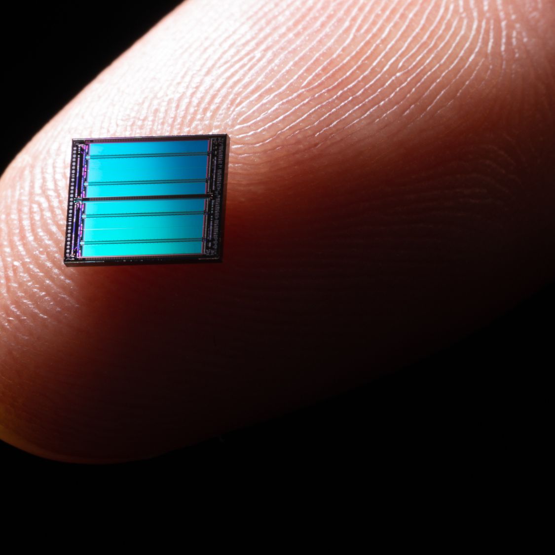
Achieving 2nm parity requires capital expenditure on an unprecedented scale. Building a competitive leading-edge foundry ecosystem is a multi-billion-dollar endeavor fraught with execution risks and steep depreciation schedules. The Japanese government has committed upwards of 4 trillion yen ($26+ billion) in direct subsidies, R&D grants, and loan guarantees to revitalize domestic chip manufacturing.
Crucially, this capital is not being deployed in a vacuum. Rapidus has forged strategic technological alliances with IBM—leveraging its pioneering 2nm nanosheet architecture research—and IMEC, the premier European nanoelectronics research hub. Furthermore, domestic equipment manufacturers like Tokyo Electron (TEL) and screen manufacturers are co-developing specialized tooling optimized for high-yield 2nm fabrication.
| Metric / Parameter | Legacy Japanese Industry Standard | New 2nm Initiative (Rapidus / Ecosystem) | Global Industry Benchmark (TSMC / Intel) |
|---|---|---|---|
| Minimum Feature Node | 40nm - 28nm (Mature Logic) | 2nm GAA Nanosheet | 2nm / 18A Class |
| State Subsidies (Yen / USD) | Nominal / Fragmented | ¥4 Trillion+ ($26B+ USD) | Varies (CHIPS Act / EU Chips Act) |
| Pilot Line Operational Target | Historical / Outdated | 2025 (Chitose, Hokkaido Fab) | 2024 - 2025 |
| Commercial Scaling | N/A | 2027 | 2025 - 2026 |
Industry & Market Implications: Winners and Losers
The resurgence of Japan as a 2nm semiconductor contender introduces complex dynamics across global equity markets and supply chains. Understanding these shifts is vital for institutional investors managing asset allocation and risk mitigation.
The Winners
- Japanese Semiconductor Equipment & Materials Providers: Companies specializing in extreme ultraviolet (EUV) photoresists, silicon wafers, and precision etching tools are experiencing surging order books and expanding valuation multiples.
- Enterprise Cloud Providers & AI Hyperscalers: Diversification of foundry sources reduces geopolitical single-point-of-failure risk, ensuring steady hardware pipelines for data center expansion.
- The Japanese Industrial Complex: Automotive and robotics conglomerates gain preferential, secure access to cutting-edge domestic compute infrastructure, insulating them from foreign export controls and supply crunches.
The Losers and Challengers
- Concentrated Foundries: While Taiwan and South Korea maintain a first-mover advantage, the emergence of a well-funded, state-backed Japanese competitor introduces long-term pricing pressure and challenges absolute market share dominance.
- Legacy Fabless Designers Relying on Single-Source Nodes: Companies slow to adopt multi-sourcing strategies may face margin contraction as foundry capacity tightens globally.
Frequently Asked Questions (People Also Ask)
What is Rapidus and what is its role in Japan's 2nm chip strategy?
Rapidus is a Japanese semiconductor manufacturing enterprise established in 2025 with backing from major corporations (including Toyota, Sony, and SoftBank) and extensive government subsidies. Its primary mandate is to establish domestic mass production of advanced 2nm gate-all-around (GAA) logic chips by 2027, restoring Japan's leadership in leading-edge semiconductor fabrication.
Why are 2nm semiconductor chips considered critical for enterprise AI and cloud architecture?
2nm chips utilize advanced GAA nanosheet architectures that offer dramatically higher transistor density, lower power leakage, and superior energy efficiency compared to older nodes. This translates directly into reduced data center operational expenditures (OpEx), faster AI model training times, and improved enterprise ROI on massive IT infrastructure investments.
How is Japan funding its multi-billion-dollar semiconductor revival?
The Japanese government, through the Ministry of Economy, Trade and Industry (METI), has allocated over 4 trillion yen ($26 billion USD) in direct subsidies, tax incentives, and loan guarantees. This public capital is augmented by private equity contributions from Japan’s leading automotive, financial, and technology conglomerates.
When will Japan's 2nm chips be available for commercial deployment?
Pilot manufacturing lines at the Rapidus facility in Chitose, Hokkaido, are slated to operationalize in 2025. Following rigorous yield optimization and customer sample testing, high-volume commercial scaling and mass production are targeted for 2027.
Future Outlook and Key Milestones to Watch
As the global technology industry looks toward 2027, Japan’s 2nm initiative represents a fascinating intersection of aggressive industrial policy, materials science excellence, and geopolitical risk mitigation. While execution risk remains high—particularly regarding production yields, equipment calibration, and talent acquisition—the structural momentum behind Rapidus and its partners cannot be understated.
For enterprise decision-makers, institutional investors, and technology strategists, the critical milestones to monitor over the next 24 to 36 months include:
- Pilot Line Yield Stability (2025–2026): Verification of defect densities and electrical performance characteristics at the Hokkaido fabrication plant.
- Global Customer Adoption & Design Wins: Announcements of major fabless design contracts from US, European, and domestic hyperscalers committing to the 2nm platform.
- Upstream Supply Chain Integration: Continued R&D breakthroughs in advanced packaging and EUV lithography tooling cooperation between domestic suppliers and international partners.
Should Japan successfully execute its roadmap, the global semiconductor landscape will transition from a fragile tri-region oligopoly to a fiercely contested multi-polar market—fundamentally altering how enterprise compute infrastructure is sourced, secured, and scaled for the artificial intelligence era.