As the artificial intelligence boom strains global electrical grids and pushes silicon manufacturing to atomic extremes, the race to commercialize 2-nanometer (2nm) chip architectures has shifted from a theoretical race to a high-stakes corporate battlefield. According to strategic analysis released by The Futurum Group on February 11, 2026, material science innovations spearheaded by Applied Materials represent a fundamental pivot point for the entire semiconductor ecosystem. With enterprise software workloads demanding exponential increases in compute capacity, the industry’s ability to transition from FinFET to Gate-All-Around (GAA) and emerging CFET designs will dictate the future trajectory of enterprise AI chips.
The 2nm Physics Crisis: Why Material Science Now Dictates Geopolitics
For decades, Moore’s Law marched forward on the promise of lithographic scaling. However, as fabrication nodes shrink toward 2nm and below, quantum tunneling, parasitic capacitance, and severe thermal dissipation threaten to halt silicon evolution entirely. At this microscopic scale, traditional planar and early FinFET structures leak current uncontrollably, rendering hyper-dense AI accelerators inefficient and economically unviable for widespread enterprise deployment.
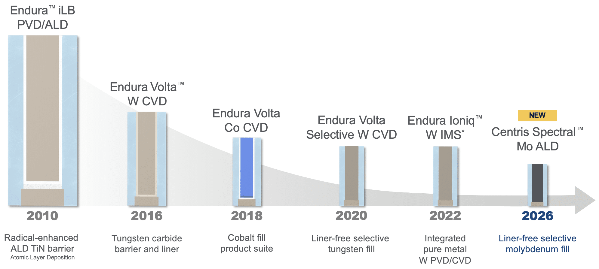
This technical impasse has elevated equipment suppliers like Applied Materials to the center of global macroeconomic policy and capital allocation strategies. Fabless AI leaders, hyperscale cloud providers, and sovereign compute initiatives are no longer constrained merely by design capability, but by the physical limits of materials engineering. The core challenge lies in depositing atomic-scale films with absolute precision—a domain where Applied Materials has introduced revolutionary selective deposition and material modification tool-sets.
Decoding Applied Materials' Transistor Breakthroughs
The recent findings highlighted by analyst Brendan Burke emphasize that Applied Materials is successfully addressing the multi-layered hurdles of GAA nanosheet integration. In a GAA transistor, the gate completely surrounds the channel, offering vastly superior electrostatic control compared to FinFETs. Yet, manufacturing these complex, ribbon-like structures requires unprecedented atomic-level precision.
Applied Materials’ latest innovations focus on three primary technological pillars:
- Selective Epitaxy and Deposition: Enabling defect-free growth of silicon-germanium channels that dictate carrier mobility and overall switching speed in 2nm nodes.
- Advanced Planarization and Chemical Mechanical Polishing (CMP): Mitigating topographical variations across 300mm wafers to ensure uniform gate lengths and predictable electrical characteristics.
- EUV Patterning Films: Deploying specialized hardmasks and metal oxide resists that withstand extreme ultraviolet radiation without line-edge roughness degradation.
These breakthroughs directly target power-performance-area (PPA) metrics, offering up to a 30% reduction in power consumption at equivalent clock speeds compared to standard 3nm iterations. For enterprise data centers grappling with astronomical power bills and cooling expenditures, this efficiency gain translates directly into enhanced enterprise ROI and improved cloud compute architecture economics.
Comparative Technical & Market Metrics
To contextualize the magnitude of this shift, the following table breaks down the transition from legacy FinFET nodes to advanced 2nm GAA architectures, highlighting the performance metrics and financial risk factors driving industry adoption:
| Metric / Parameter | Legacy FinFET (5nm / 4nm) | Current Generation (3nm) | Next-Gen 2nm GAA (Applied Materials Focus) |
|---|---|---|---|
| Gate Control Topology | Three-sided Fin | Fin / Early Nanosheet Hybrid | Full Gate-All-Around (GAA) Nanosheet |
| Power Efficiency Gain | Baseline (1x) | 15% - 20% Improvement | Up to 30% Improvement over 3nm |
| Wafer Fab Equipment (WFE) Intensity | Moderate Capital Expenditure | High Capital Expenditure | Ultra-High; Requires Specialized Deposition Tools |
| Enterprise ROI Impact | Standard Depreciation Curves | Extended Payback Periods | Accelerated Payback via Power Density Optimization |
Industry & Market Implications: Winners, Losers, and Capital Allocation
The commercial rollout of 2nm AI chips supported by Applied Materials' tool ecosystem triggers immediate ripples across global financial markets. Foundries that successfully integrate these material breakthroughs will capture outsized market share, commanding premium wafer pricing and expanding their gross margins. Conversely, competitors lagging in GAA yield stabilization face severe margin compression and diminished valuation multiples.
From a risk mitigation perspective, major cloud service providers and AI hardware designers are actively diversifying their foundry partnerships. However, because Applied Materials holds a dominant position in material engineering and selective deposition equipment, the company effectively acts as a toll-booth for the entire generation of 2nm silicon. This market liquidity and pricing power reinforce robust cash flow projections, insulating the firm against cyclical downturns in consumer electronics.
Regulatory compliance and geopolitical export controls also cast a complex shadow over these developments. As advanced semiconductor manufacturing equipment remains subject to stringent trade restrictions, tool-makers must navigate fragmented regional supply chains while protecting intellectual property and maintaining operational efficiency.
Frequently Asked Questions (People Also Ask)
What makes Applied Materials' transistor breakthroughs crucial for 2nm AI chips?
Applied Materials provides the advanced materials engineering, selective deposition, and planarization tools required to manufacture Gate-All-Around (GAA) nanosheet transistors. These tools overcome severe quantum leakage and thermal limits, allowing 2nm chips to deliver higher compute density and superior energy efficiency for intensive AI workloads.
How do 2nm GAA chips impact enterprise ROI and data center infrastructure?
By reducing power consumption by up to 30% compared to previous nodes while boosting processing performance, 2nm GAA chips alleviate the massive cooling and electricity burdens facing modern data centers. This efficiency directly improves enterprise ROI by lowering total cost of ownership (TCO) for large-scale AI model training and inference.
What are the primary manufacturing challenges in transitioning to 2nm nodes?
The primary hurdles include controlling atomic-scale film thickness, preventing parasitic capacitance, mitigating wafer defects during epitaxial growth, and managing extreme thermal dissipation within multi-layer nanosheet structures.
How does this technological advancement affect semiconductor capital expenditure and valuation multiples?
The extreme complexity of 2nm fabrication drives higher Wafer Fab Equipment (WFE) intensity. Foundries must commit substantial capital expenditure to upgrade tool-sets, which in turn supports premium valuation multiples for foundational equipment suppliers like Applied Materials that hold monopolistic control over critical deposition steps.
Future Outlook & Milestones to Watch
As the industry moves through 2026 and toward volume production in 2027, several key milestones will determine the ultimate success of Applied Materials' 2nm initiatives. Analysts will closely monitor foundry yield reports, initial high-volume manufacturing (HVM) tape-outs from major fabless designers, and the pace of tool installations across major fabrication hubs in Taiwan, the United States, and South Korea.
Ultimately, Applied Materials has positioned itself not merely as a equipment vendor, but as an indispensable architect of the next era of enterprise intelligence. For investors, enterprise IT leaders, and policymakers alike, monitoring the execution velocity of these transistor innovations will remain paramount to navigating the evolving global technology landscape.