India Unleashes ₹1.27 Lakh Crore 'Semicon 2.0' Mega-Package: Inside New Delhi's $48 Billion Gamble to Break the Global Silicon Oligopoly
Executive Takeaways
- Unprecedented Sovereign Outlay: The Union Cabinet has ratified Semicon India 2.0 with a landmark fiscal commitment of ₹1.27 lakh crore (~$15.2 billion), superseding the inaugural ₹76,000 crore framework to address acute midstream and supply chain dependencies.
- Massive Capital Multiplier: New Delhi models the expanded incentive architecture to crowd in an estimated ₹4 lakh crore (~$48 billion) in cumulative public-private capital expenditure across commercial fabrication, advanced OSAT/ATMP, and raw substrate materials.
- Pivot to Full-Stack Localization: Unlike the assembly-heavy posture of the initial phase, Phase 2.0 aggressively subsidizes domestic supply chain inputs, chemical purity infrastructure, equipment manufacturing, and indigenous deep-tech IP under an overhauled Design-Linked Incentive (DLI) mechanism.
- Geopolitical Supply-Chain Recalibration: The package directly positions India as an indispensable node for Western and Indo-Pacific enterprise resilience, de-risking global cloud compute architectures, defense avionics, and automotive supply chains from East Asian geopolitical choke points.
The Geopolitical & Macroeconomic Gambit: Beyond Assembly into Core Silicon
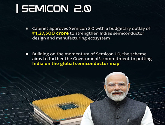
In what marks the most consequential industrial policy realignment in modern Asian economic history, the Union Cabinet, chaired by the Prime Minister, has formally ratified the execution of Semicon India 2.0. Armed with a direct state commitment of ₹1.27 lakh crore, the revised doctrine expands India's baseline ambition from an opportunistic outsourced assembly and testing hub into an integrated, vertically localized semiconductor powerhouse.
The sovereign intervention arrives at a defining inflection point for the global merchant silicon complex. As hyperscale cloud providers, enterprise hardware manufacturers, and automotive original equipment manufacturers (OEMs) scramble to insulate their forward balance sheets against localized Pacific rim disruptions, the cost of supply chain redundancy has surged to premium levels. India's latest capital allocation is explicitly structured to bridge the enterprise ROI gap that has traditionally disadvantaged greenfield manufacturing environments compared to legacy foundry clusters in Taiwan, South Korea, and the Yangtze River Delta.
Under the initial ₹76,000 crore tranche, India secured milestone wins—most notably Micron Technology’s assembly, testing, marking, and packaging (ATMP) footprint in Sanand, Gujarat, followed by commercial fabrication joint ventures spearheaded by Tata Electronics alongside Taiwan’s Powerchip Semiconductor Manufacturing Corporation (PSMC) at Dholera, alongside critical OSAT developments by the Murugappa Group, Renesas, and Kaynes SemiCon. Yet, internal policy audits conducted across 2025 indicated that without addressing the foundational layers of the industrial pyramid—namely specialized gases, photolithography chemicals, silicon ingot processing, and intellectual property (IP) design ownership—the country's domestic value addition would remain vulnerable to foreign embargoes and global allocation shocks.
Capital Architecture: Deconstructing the ₹1.27 Lakh Crore Allocation
The structural engineering of Semicon India 2.0 reflects a marked maturation in statecraft and corporate risk mitigation. Rather than distributing fiscal relief evenly across speculative bids, the Ministry of Electronics and Information Technology (MeitY) and the India Semiconductor Mission (ISM) have calibrated the expanded funds across four high-leverage verticals designed to optimize capital allocation and operational velocity:
- Commercial Wafer Fabs (Trailing & Mature Nodes): Dedicated capex support maintaining up to 50% central fiscal parity on a pari-passu basis, aggressively targeting 28nm to 65nm nodes essential for industrial robotics, EV powertrains, smart grid controllers, and edge-telecom gear.
- Advanced Packaging, ATMP & 3D Heterogeneous Integration: Transitioning incentives from basic wire-bonding assembly toward high-margin wafer-level packaging, silicon photonics integration, and panel-level packaging required by next-generation enterprise AI accelerators.
- Upstream Supply Chain & Chemical Ecosystem: A distinct carve-out subsidizing local production of ultra-pure hydrogen peroxide, electronic-grade silane, photoresists, quartz ware, and specialized polysilicon, directly dismantling the 100% import reliance on foreign chemical monopolies.
- Overhauled DLI 2.0 (Design-Linked Incentives): Elimination of restrictive IP-transfer caps, allowing venture-backed Indian fabless startups access to sovereign-subsidized compute clusters, EDA tools from Synopsys and Cadence, and Multi-Project Wafer (MPW) runs to retain equity value onshore.
By underwriting upfront capital intensity, New Delhi calculates that the ₹1.27 lakh crore sovereign anchor will catalytically mobilize roughly ₹4 lakh crore in parallel corporate balance-sheet outlays. This leverage ratio rests on underwriting enterprise-grade risk, ensuring that participating multinationals achieve acceptable valuation multiples while building out redundant multi-billion-dollar foundries.
Verified Data Breakdown: Structural Shift Across Policy Tranches
The transition from Semicon India 1.0 to 2.0 signals a transition from initial ecosystem validation to industrial scale-out. The structural variations between the two programmatic phases are delineated below:
| Policy Dimension | Semicon India 1.0 (2021–2025) | Semicon India 2.0 (Ratified July 2026) | Strategic & Financial Impact |
|---|---|---|---|
| Direct Budgetary Outlay | ₹76,000 Crore (~$9.1B) | ₹1,27,000 Crore (~$15.2B) | +67.1% sovereign resource expansion; institutionalizes the India Semiconductor Mission. |
| Projected Capex Mobilization | ₹1.50 to ₹1.80 Lakh Crore | ₹4,00,000 Crore (~$48B) | Deepens private market liquidity and cross-border syndicated debt participation. |
| Subsidized Core Focus | Front-end fabs and baseline OSAT packaging facilities. | Trailing-edge fabs, compound silicon (SiC/GaN), specialized chemicals, advanced packaging. | Mitigates tier-3 supply chain risks; establishes sovereign resilience against raw material chokepoints. |
| Design-Linked Scope (DLI) | Capped incentives; strictly monitored IP domicile limits. | Compute infrastructure credits, EDA site licensing access, global IP commercialization parity. | Elevates enterprise ROI for domestic fabless chip developers and venture capital pools. |
| Domestic Value Capture (Target) | Estimated at 10% to 15% (heavily assembly-centric). | Targeted at 35% to 45% across fab materials, chemical inputs, and packaging. | Protects long-term foreign exchange reserves while scaling high-complexity manufacturing jobs. |
Industry & Enterprise Implications: Market Winners, Losers, and Capex Friction
The aggressive expansion of Semicon India 2.0 sends ripples across the global tech equity landscape, reallocating capital expenditure flows across public and private enterprise domains.
The Winners: Enterprise Titans and Tier-1 Infrastructure Providers
The clearest beneficiaries of the ₹1.27 lakh crore injection are industrial conglomerates with capitalized balance sheets and institutional access to massive power and water infrastructure. Tata Electronics, with its foundational investments in both Dholera (Fab) and Jagiroad (OSAT), sits at the center of this capital deployment, drastically reducing its long-term amortization costs. Similarly, integrated packaging operators like Micron Technology, alongside joint ventures involving Renesas Electronics and the Murugappa Group's CG Power, gain expanded visibility into second-tier supplier subsidies, accelerating their margin progression toward operational breakeven.
Beyond the semiconductor manufacturers themselves, high-purity industrial infrastructure providers, utility scale renewable developers, and precision engineering specialists will capture outsized tailwinds. Enterprise automation platforms, cleanroom construction conglomerates, and global EDA (Electronic Design Automation) software providers stand to secure expanded recurring enterprise licensing revenues through the government-subsidized DLI pipeline.
The Losers: Legacy Assemblers and Uncapitalized Market Entrants
Conversely, low-tier electronics manufacturing services (EMS) providers that have relied entirely on basic surface-mount technology (SMT) and rudimentary screw-to-fit assembly will face strategic displacement. As global regulatory compliance frameworks (such as the EU Corporate Sustainability Due Diligence Directive and tightening US supply-chain provenance mandates) demand verifiable end-to-end component traceability, simple contract box-builders that fail to integrate vertically into advanced testing or component fabrication will see valuation multiples compress.
Furthermore, fabless design startups that lack differentiated, enterprise-ready intellectual property face intense capital rationalization. While Semicon 2.0 subsidizes design and prototyping toolsets, the state has tied later-stage fiscal disbursements to validated commercial production milestones—a policy pivot designed to wash speculative paper-only architectures out of the state incentive funnel.
Frequently Asked Questions (People Also Ask)
What is the core difference between Semicon India 1.0 and Semicon India 2.0?
Semicon India 1.0 focused primarily on establishing proof-of-concept by attracting anchor tenants through a ₹76,000 crore incentive package targeting front-end commercial foundries and OSAT/ATMP units. Semicon India 2.0 scales the sovereign commitment to ₹1.27 lakh crore, deliberately targeting the broader ecosystem: upstream raw materials, specialty chemical manufacturing, compound semiconductors (Silicon Carbide and Gallium Nitride), domestic fabless IP, and the equipment supply chain required to achieve higher localized value addition.
How will the ₹1.27 lakh crore program generate ₹4 lakh crore in investments?
The government acts as a sovereign co-investor rather than a primary financier. By offering up to 50% capital expenditure subsidies alongside complementary state-level infrastructure incentives (subsidized land, water, renewable power, and tax credits), the program materially alters the internal rate of return (IRR) for private enterprise. This de-risking mechanism encourages global chip giants, Indian industrial conglomerates, and sovereign wealth vehicles to commit the remaining 50% to 60% of required capex from private balance sheets and syndicated credit facilities.
Why is India prioritizing legacy nodes (28nm to 65nm) instead of cutting-edge 3nm/2nm chips?
While sub-5nm fabrication dominates high-profile smartphones and data-center AI GPUs, roughly 70% of global industrial, automotive, telecommunications, defense, and power grid components operate on mature nodes (28nm and above). These nodes carry significantly lower capital intensity, proven yields, longer economic life cycles, and immediate domestic absorption within India’s rapidly accelerating automotive and consumer electronics manufacturing bases, providing a far more realistic and predictable enterprise ROI.
How does Semicon India 2.0 impact global semiconductor supply chain diversification?
Global corporations are aggressively executing "China+1" and "Taiwan-hedge" supply chain doctrines. By building state-backed, geographically secure foundry and advanced packaging capacity along key logistics corridors, India offers global OEMs an alternative manufacturing node that mitigates geopolitical chokepoints, secures cloud compute architectures, and prevents future enterprise revenue losses driven by microchip allocations.
Strategic Horizon: Critical Milestones to Watch (2026–2030)
As the administrative machinery transitions from legislative ratification to balance-sheet capital deployment, enterprise markets will assess the efficacy of Semicon India 2.0 against explicit operational milestones:
- Commercial Silicon Yields (2026–2027): The initial commercial wafer outs from the Dholera facility and pilot packaging volumes from the Sanand and Morigaon sites will serve as the premier viability test for global foundry customers assessing defect densities and international operational benchmarks.
- Upstream Chemical Integration (2027–2028): The deployment of capital within the newly subsidized chemical and gas verticals will determine whether India can lower its bill-of-materials import dependency from over 90% to below 60%.
- Domestic Fabless Commercialization (2028–2030): The metric of success for DLI 2.0 will center on whether an Indian-domiciled fabless architectural firm achieves a tier-1 global hyperscaler design win, securing a sovereign path from tape-out to commercial deployment.
The Cabinet’s approval of ₹1.27 lakh crore confirms that New Delhi no longer views microelectronics merely as a trade balance challenge, but as an existential component of national sovereignty and macroeconomic stability. The next four years will establish whether this sovereign capital deployment can successfully convert ambitious industrial blueprints into operational, globally competitive silicon output.
!['Mirzapur: The Movie' box office collection Day 2 [LIVE]: Pankaj Tripathi, Ravi Kishan, and Ali Fazal sta](https://static.toiimg.com/thumb/resizemode-4,width-1280,height-720,msid-133797053/133797053.jpg)