Executive Takeaways
- Strategic Alliance: IBM and newly formed Japanese foundry Rapidus signed a landmark agreement on December 12, 2022, to jointly develop 2-nanometer (nm) gate-all-around (GAA) nanosheet semiconductor technology.
- National Sovereignty Play: Backed by billions in direct capital allocation from the Japanese Ministry of Economy, Trade and Industry (METI), Rapidus aims to restore domestic commercial production of leading-edge logic chips, reducing acute supply chain vulnerabilities.
- Technological Foundation: The partnership leverages IBM Research’s proven 2nm node breakthrough—announced in May 2021—accelerating infrastructure scalability and bridging the gap between laboratory physics and commercial manufacturing.
- Market Disruption: This public-private enterprise redefines the global foundry landscape, challenging the Taiwanese and South Korean duopoly (TSMC and Samsung) while realigning U.S.-Japan technological security frameworks.
In the high-stakes theater of global semiconductor manufacturing, geography is destiny, and capital allocation is the ultimate weapon of economic statecraft. On December 12, 2022, International Business Machines Corporation (IBM) and Rapidus Corporation—a freshly minted, government-backed Japanese semiconductor consortium—announced a strategic partnership that fundamentally alters the geopolitical architecture of advanced microelectronics. Designed to industrialize IBM’s pioneering 2-nanometer (nm) gate-all-around (GAA) nanosheet technology in Japan, this alliance is far more than a routine corporate licensing deal. It represents a sovereign industrial mobilization, a calculated hedge against acute geopolitical risk in the Taiwan Strait, and a bold attempt to resurrect Japan’s once-dominant semiconductor manufacturing hegemony.
For enterprise leaders, institutional investors, and tech sector strategists, the IBM-Rapidus pact offers a fascinating case study in risk mitigation, cross-border technology transfer, and public-private capital deployment. As global enterprises grapple with enterprise ROI pressures, supply chain resilience, and rigorous regulatory compliance, understanding the mechanics, financial backing, and long-term implications of this partnership is essential for forecasting the next decade of digital infrastructure development.
The Catalytic Catalyst: Why Japan is Re-Entering the Leading-Edge Fray
Test Our Free AI & Tech Utilities Suite
Calculate LLM API token costs, analyze article dwell-time, or simulate tech DCA returns.
To fully grasp the magnitude of the December 2022 announcement, one must examine the structural vulnerabilities exposed by the post-pandemic global supply chain crisis. For decades, Japan maintained a commanding position in semiconductor materials and manufacturing equipment—supplying vital photoresists, silicon wafers, and lithography components to the global market. However, following the contraction of its domestic dynamic random-access memory (DRAM) and logic fabrication sectors in the late 1990s and 2000s, Japan largely ceded sub-10nm logic manufacturing to Taiwan Semiconductor Manufacturing Company (TSMC), Samsung Electronics, and Intel.
This heavy reliance on offshore foundries created a structural vulnerability for Japanese industrial conglomerates, automakers, and digital infrastructure providers. Recognizing this existential risk, the Japanese government—spearheaded by METI—embarked on a massive industrial policy pivot. Tokyo committed nearly 1 trillion yen ($7.5 billion USD at the time) in subsidies to rebuild domestic semiconductor capabilities, attracting TSMC to build a mature-node fab in Kumamoto while simultaneously orchestrating the creation of Rapidus.
Formed in August 2022 with backing from corporate heavyweights including Toyota, Sony, NTT, SoftBank, Kioxia, Denso, NEC, and MUFG Bank, Rapidus was engineered specifically to bridge the gap between advanced research and commercial mass production. Yet, Rapidus faced a formidable barrier to entry: leaping straight from legacy nodes to the bleeding edge of 2nm technology without an existing foundational process design kit (PDK) or high-volume manufacturing (HVM) footprint. Enter IBM.
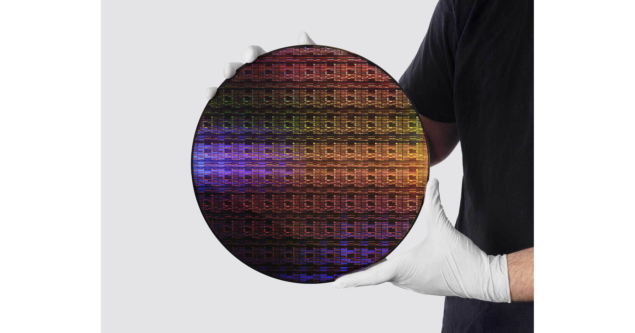
In May 2021, IBM Research made waves across the global technology sector by unveiling the world’s first 2nm nanosheet technology. By packing 50 billion transistors onto a fingernail-sized chip, IBM demonstrated that its architectural innovations could deliver a 45% performance increase or a 75% energy efficiency boost compared to prevailing 7nm commercial nodes. By partnering with IBM, Rapidus bypassed years of foundational R&D, acquiring immediate access to process architecture that would otherwise require billions in independent capital expenditure.
Decoding the Technology: 2nm GAA Nanosheets and Infrastructure Scalability

The core of the IBM-Rapidus agreement centers on the commercialization of gate-all-around nanosheet transistor architecture. As semiconductor scaling approached the physical limits of traditional FinFET (Fin Field-Effect Transistor) designs at the 3nm and 2nm thresholds, leakage current and short-channel effects threatened to halt Moore’s Law.
IBM’s 2nm nanosheet design solves this physics dilemma by replacing vertical fins with horizontal ribbons of silicon stacked within each transistor channel. This configuration allows gate material to completely wrap around the channel, exerting precise electrostatic control over current flow. For enterprise cloud compute architecture, this translates to game-changing efficiency gains:
- Server Power Optimization: Data center operators facing soaring electricity costs and ESG regulatory compliance mandates can deploy servers powered by 2nm processors, drastically cutting cooling and power consumption footprints.
- Mobile and Edge Compute: Consumer electronics and Internet of Things (IoT) devices manufactured on the Rapidus-IBM node will experience quadruple battery life extensions, enabling prolonged untethered operations for advanced AI inference at the edge.
- High-Performance Computing (HPC): Supercomputing workloads, financial modeling, and complex cryptographic processing will benefit from accelerated execution speeds without exceeding thermal design power (TDP) thresholds.
However, translating laboratory breakthroughs into commercial manufacturing lines requires flawless capital allocation and rigorous execution. Rapidus announced plans to dispatch Japanese engineers directly to IBM’s Albany Nanotech Complex in New York—a premier semiconductor R&D hub—to master the intricacies of 2nm fabrication before bringing operational lines online in Northern Japan (specifically targeting Fukushima Prefecture for pilot production by 2025 and mass production by the late 2020s).
Verified Data & Metrics Breakdown
| Metric / Parameter | IBM Baseline (May 2021) | Rapidus Commercialization Target | Strategic Implication |
|---|---|---|---|
| Node Architecture | 2nm GAA Nanosheet | 2nm GAA Nanosheet (Production) | Bypasses legacy FinFET nodes; jumps straight to next-gen logic. |
| Transistor Density | 50 Billion Transistors / Chip | Volume Production Equivalent | Enables unprecedented on-die AI processing power. |
| Performance vs. 7nm | +45% Performance / -75% Power | Commercial Parity | Reduces carbon footprint and power overhead for enterprise data centers. |
| Public/Private Funding | N/A (Proprietary R&D) | ~¥1 Trillion+ (METI & Corporate) | Guarantees baseline solvency and long-term infrastructure runway. |
| Timeline to HVM | 2021 (Lab Demonstration) | Pilot 2025 / Mass Production 2027 | Aggressive execution schedule challenging established foundry timelines. |
Industry & Market Implications: Winners, Losers, and Economic Realities
The formation of the IBM-Rapidus partnership sends powerful shockwaves through the global semiconductor ecosystem, redrawing competitive boundaries across Wall Street, Tokyo, Taipei, and Washington.
The Winners:
- IBM: By monetizing its intellectual property portfolio through strategic licensing and joint development agreements, IBM solidifies its status as a foundational architect of enterprise compute, generating high-margin technology transfer revenue without assuming heavy foundry capital expenditure risks.
- The Japanese Industrial Complex: Automotive giants (Toyota), industrial automation leaders, and telecommunications firms regain a secure domestic supply chain for critical logic semiconductors, insulating them from geopolitical disruptions in the Taiwan Strait.
- Semiconductor Equipment Manufacturers: Japanese tool makers (such as Tokyo Electron) and international lithography suppliers stand to secure lucrative equipment sales as Rapidus constructs its greenfield fabrication facilities.
The Losers and Challenges:
- Established Foundry Incumbents (TSMC and Samsung): While TSMC maintains an immense manufacturing scale and process maturity advantage, the emergence of a well-funded, sovereign-backed competitor in Japan introduces long-term diversification pressure from major fabless clients seeking multi-source foundry options.
- Execution Risk Bearers: Rapidus faces an exceptionally steep hill to climb. Scaling from laboratory process design to high-yielding, high-volume commercial manufacturing within a five-year window has historically tested even the most experienced semiconductor operators (as observed with Intel’s historical node transitions). Capital burn rates and valuation multiples will be heavily scrutinized by participating Japanese financial institutions.
Frequently Asked Questions (People Also Ask)
1. What is the core objective of the IBM and Rapidus partnership?
The primary objective is to jointly develop and commercialize IBM’s breakthrough 2-nanometer gate-all-around (GAA) nanosheet semiconductor technology in Japan. Rapidus aims to establish advanced, domestic leading-edge logic chip manufacturing capabilities to secure supply chain resilience and revitalize Japan’s semiconductor industry.
2. How is the Rapidus manufacturing initiative funded?
Rapidus is backed by significant public-private capital allocation. The Japanese government, through the Ministry of Economy, Trade and Industry (METI), has committed roughly 1 trillion yen ($7.5+ billion USD) in subsidies. Additionally, a consortium of major Japanese corporations—including Toyota, Sony, NTT, SoftBank, and MUFG Bank—provides foundational private equity and strategic backing.
3. Why is 2nm GAA nanosheet technology important for enterprises?
2nm GAA technology offers up to a 45% performance increase and a 75% power efficiency improvement compared to 7nm chips. For enterprise organizations, this translates to massive energy savings in hyperscale data centers, reduced cloud infrastructure cooling costs, and enhanced processing power for artificial intelligence (AI) and machine learning workloads.
4. When is Rapidus expected to begin mass production of 2nm chips?
Rapidus has outlined an aggressive operational roadmap, targeting pilot line production and technology transfer validation by 2025, with full-scale commercial mass production slated for the late 2020s (approximately 2027).
Future Outlook: Milestones to Watch
As the ink dries on the IBM-Rapidus agreement, the spotlight shifts from diplomatic handshakes to rigorous operational execution. For market analysts and institutional investors, several critical milestones will determine whether this ambitious public-private venture achieves commercial viability:
- Success of Engineer Training Programs: Monitor the velocity and knowledge-transfer metrics of Japanese engineers deployed to IBM’s Albany Nanotech Complex. The ability to successfully absorb and adapt complex 2nm process recipes is the foundational prerequisite for success.
- Fab Construction and Tool Installation: Track construction progress on Rapidus’ dedicated manufacturing facility (dubbed IIM - Innovative Integration for Manufacture) in Hokkaido, Japan, alongside delivery schedules for extreme ultraviolet (EUV) lithography systems from ASML.
- Customer Acquisition and Ecosystem Buy-In: Evaluate whether Rapidus can secure binding commitments from major global fabless chip designers (such as Apple, NVIDIA, or Qualcomm) or if its initial output will remain primarily dedicated to domestic Japanese automotive and industrial conglomerates.
Ultimately, the IBM-Rapidus alliance is a watershed moment in industrial policy and technology geopolitics. By fusing American foundational R&D with Japanese manufacturing discipline and state-backed capital, this partnership serves as a masterclass in strategic risk mitigation. Whether it succeeds in permanently altering the global foundry duopoly remains one of the most compelling narratives in modern finance and technology.