NEW YORK & ALBANY — In an industry where microscopic fractions of a nanometer dictate global macroeconomic balances, geopolitical leverage, and corporate valuation multiples, International Business Machines (IBM) delivered a tectonic shockwave. On May 6, 2021, IBM Research announced the successful fabrication and testing of the world’s first 2-nanometer nanosheet semiconductor. Housed within the ultra-clean rooms of the Albany NanoTech Complex, this fingernail-sized piece of silicon packed an unprecedented 50 billion transistors.
For financial markets, corporate boardrooms, and cloud compute architects, the announcement was far more than an academic triumph of materials science. It represented a direct challenge to the physical limits of Moore’s Law and a masterclass in risk mitigation for a tech sector choked by severe supply chain vulnerabilities. As enterprise capital expenditure increasingly prioritizes energy-efficient data center operations over brute-force silicon density, IBM’s 2nm architecture has emerged as a blueprint for the next decade of digital infrastructure.
The Catalytic Catalyst: Escaping the Thermal Wall
To understand the profound market implications of IBM’s May 2021 disclosure, one must examine the physical crisis gripping the semiconductor manufacturing sector at the turn of the decade. By 2021, commercial deployments had largely settled into the 7nm and nascent 5nm nodes. However, engineers were rapidly slamming into the "thermal wall"—a point at which driving more electrical current through shrinking gates yields diminishing computational returns while generating destructive heat loads.
Hyper-scale cloud operators—the likes of Amazon Web Services, Microsoft Azure, and Google Cloud—were facing spiraling power bills and stringent regulatory compliance targets regarding carbon footprints. In this environment, infrastructure scalability was no longer constrained by architectural software design, but by raw semiconductor physics.
IBM Research, operating out of its New York headquarters and research hubs globally, bypassed conventional FinFET (Fin Field-Effect Transistor) limitations by pivoting entirely to a gate-all-around (GAA) nanosheet architecture. By stacking three layers of silicon nanosheets vertically and wrapping the gate material completely around them, IBM engineers solved the sub-threshold leakage current issues plaguing sub-3nm nodes. The result was a density milestone: 50 billion microscopic switches integrated onto a footprint measuring a mere 150 square millimeters.
Inside the Metrics: Performance, Power, and Enterprise ROI
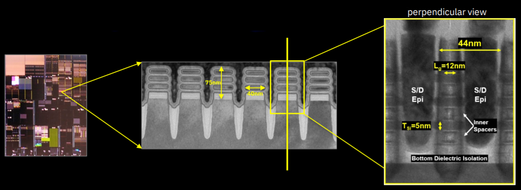
In the high-stakes realm of enterprise technology procurement, performance metrics translate directly into balance sheet profitability. IBM’s 2nm test chip metrics shattered prevailing performance benchmarks established by industry workhorses:
- Power Efficiency: Operating at the same speed as typical 7nm node chips, the 2nm architecture consumes 75% less power, slashing operational expenditure for massive server farms.
- Performance Velocity: When drawing equivalent power levels, the 2nm design delivers a 45% boost in processing speed, accelerating complex algorithmic execution for financial modeling, cryptography, and real-time machine learning inference.
- Transistor Density: Integrating 50 billion transistors into a standard form factor allows chip designers to embed specialized accelerators—such as tensor processing units and encryption engines—directly onto general-purpose server processors.
For Chief Information Officers (CIOs) and Chief Financial Officers (CFOs), these figures fundamentally alter capital allocation strategies. Upgrading server fleets with 2nm-derived processors promises to shrink server footprint requirements by up to 75%, translating into lower cooling overhead, reduced rack space leasing costs, and accelerated enterprise ROI.
Verified Data & Specifications Breakdown
TABLE 1.1: Comparative Architectural Metrics — IBM 2nm Test Chip vs. Commercial 7nm Standard (Circa 2021)
| Metric / Specification | Commercial 7nm Baseline | IBM Research 2nm Test Chip | Enterprise Financial Impact |
|---|---|---|---|
| Transistor Count | ~10 billion to 30 billion | 50 Billion | Higher functional integration per socket |
| Architectural Style | FinFET | Gate-All-Around (GAA) Nanosheet | Enhanced voltage scaling & leakage control |
| Power Reduction | Baseline (100%) | 75% Lower Power Consumption | Massive OPEX savings on data center cooling |
| Performance Gain | Baseline (100%) | +45% Speed Increase | Accelerated AI training and transaction throughput |
| Primary Target Sector | Consumer Mobile & Early Cloud | Enterprise Cloud, AI, & Edge Computing | Future-proofing core IT infrastructure |
Industry & Market Implications: Who Wins, Who Loses
The unveiling of IBM’s 2nm breakthrough sent strategic ripples through global financial markets, forcing equity analysts to re-evaluate the competitive positioning of major semiconductor pure-play foundries and integrated device manufacturers (IDMs).
The Winners: Intellectual Property Licensors and Cloud Architects
While IBM has progressively shifted its business model away from high-volume mass manufacturing—outsourcing production of its commercial Power Systems processors to partners like Samsung—its R&D engine remains a formidable tollbooth on the semiconductor highway. By proving the viability of GAA nanosheets, IBM secured cross-licensing leverage. Furthermore, hyper-scale cloud operators stand to win immensely; access to 2nm-class silicon will allow them to host denser virtual machine clusters without triggering localized grid capacity failures.
The Pressure Points: Pure-Play Foundry Hegemony
Monopoly dynamics in advanced node manufacturing—concentrated heavily between Taiwan Semiconductor Manufacturing Company (TSMC) and Samsung Electronics—faced an external validation check. Although TSMC and Samsung were actively plotting their own 2nm roadmaps, IBM’s public demonstration proved that alternative research ecosystems could successfully de-risk the transition to nanosheet technology. For venture capitalists and institutional investors, the breakthrough underscored that capital allocation toward advanced semiconductor R&D remains highly unpredictable, threatening long-term valuation multiples for lagging fabrication houses.
Geopolitical & Supply Chain Risk Mitigation
Against a backdrop of pandemic-era chip shortages and escalating Sino-American trade tensions, the geographical provenance of semiconductor research took center stage. Developed largely on U.S. soil in upstate New York, IBM’s 2nm milestone provided policymakers in Washington with tangible leverage as legislative frameworks like the CHIPS Act moved toward enactment. Securing domestic access to next-generation node architecture is viewed by national security advisors as an absolute imperative for economic sovereignty.
People Also Ask (FAQ): Expert Answers
Q: What is a nanosheet transistor, and why was it necessary for IBM’s 2nm chip?
A: Traditional FinFET transistors, which stood upright like vertical fins, encountered severe quantum tunneling and leakage current issues as gates shrank below 3nm. IBM’s nanosheet architecture replaces these fins with horizontal ribbons of silicon stacked vertically. This design allows the gate material to wrap completely around each sheet (Gate-All-Around), giving engineers precise electrostatic control over current flow, eliminating current leakage, and enabling the integration of 50 billion transistors into a microscopic footprint.
Q: How does IBM’s 2nm technology directly impact enterprise IT and cloud data center costs?
A: Data center operators face punishing operational expenditure (OPEX) driven by electricity consumption and cooling requirements. By delivering a 75% reduction in power consumption at equivalent speeds to 7nm chips, IBM’s 2nm technology allows enterprises to scale computational throughput dramatically without escalating facility power footprints. This translates directly into lower utility overhead, optimized server rack densities, and superior enterprise ROI.
Q: Does IBM manufacture these 2nm chips commercially, or do they license the technology?
A: IBM primarily operates as a research and development pioneer rather than a high-volume mass manufacturer. While the initial 2nm prototype was successfully fabricated at IBM’s Albany NanoTech research facility, commercialization typically occurs through manufacturing partnerships and technology licensing agreements. For instance, IBM has historically partnered with foundry giants like Samsung to bring its advanced R&D breakthroughs—such as nanosheet architecture—into scaled production.
Q: What are the primary downstream applications for 2nm semiconductor chips?
A: Beyond enterprise cloud servers and high-performance computing (HPC) clusters, 2nm chips are projected to revolutionize artificial intelligence (AI) model training, edge computing, autonomous vehicle neural networks, and mobile devices. In smartphones, a 2nm processor could theoretically quadruple battery life between charges, whereas in data centers, it accelerates deep learning workloads by orders of magnitude.
Future Outlook: What Comes Next and Key Milestones
As the semiconductor industry digests the long-term ramifications of IBM’s 2021 milestone, market participants are closely monitoring the transition from laboratory prototyping to high-volume commercial fabrication lines. Reaching the 2nm milestone was an unprecedented feat of physics, but yield optimization—minimizing manufacturing defects across millions of wafers—remains the ultimate commercial hurdle.
Key milestones to watch over the next market cycle include:
- Foundry Ecosystem Adoption: The rate at which major foundries incorporate GAA nanosheets into commercial production lines slated for mid-decade deployment.
- Enterprise Server Refresh Cycles: The commercial debut of enterprise-grade processors built on IBM-derived 2nm architectures by server vendors and hyperscale cloud providers.
- Regulatory & Capital Flows: The deployment of domestic subsidies under legislation like the U.S. CHIPS Act, designed to ensure that foundational research conducted in labs like Albany translates into localized manufacturing capacity.
Ultimately, IBM’s 2nm test chip has redefined the outer boundaries of silicon engineering. By proving that sub-nanometer scaling remains economically and physically viable, IBM has provided the global enterprise ecosystem with a roadmap to navigate the post-Moore’s Law era—securing the computational horsepower required to drive the global digital economy for the next decade and beyond.