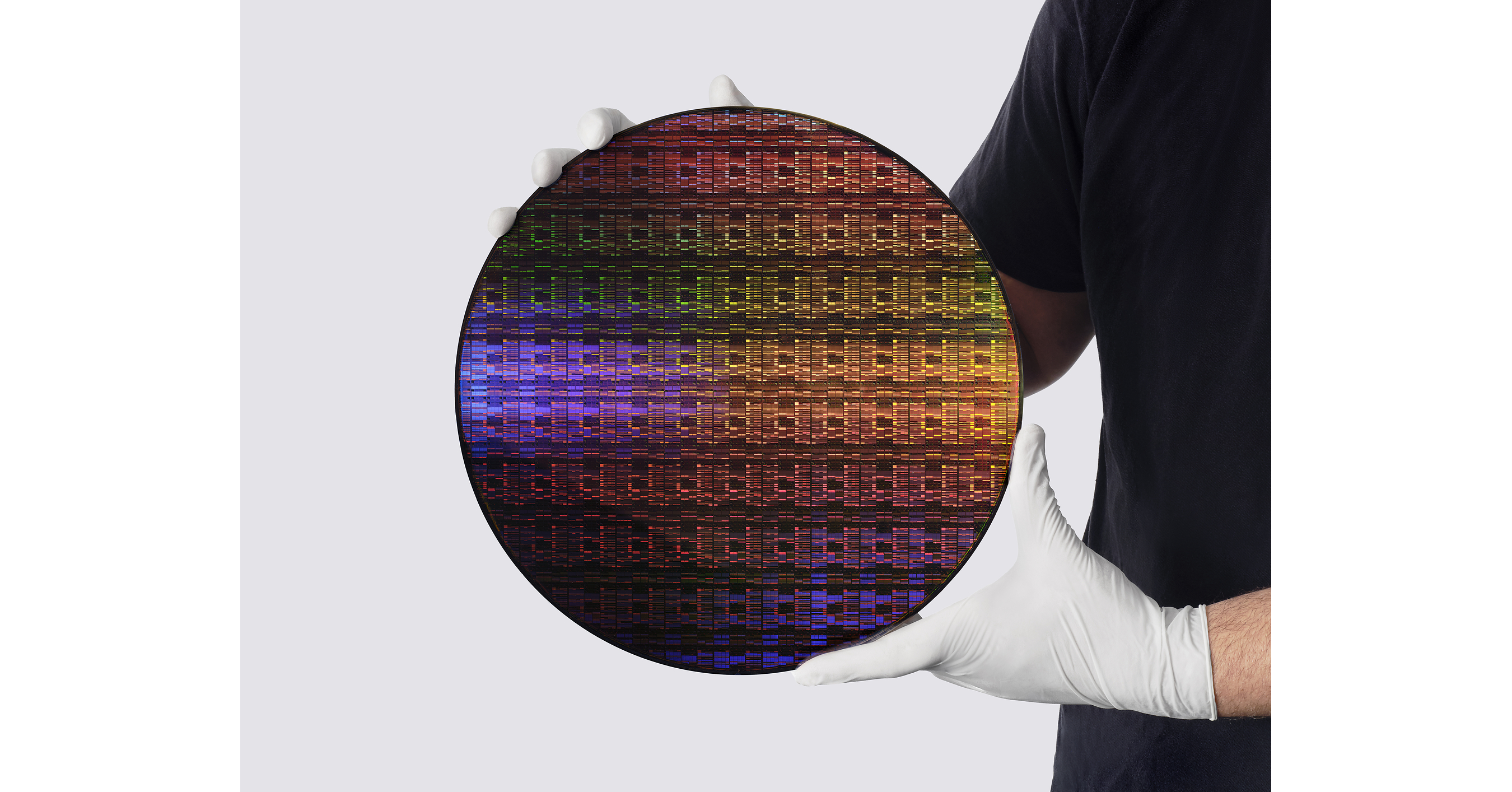
NEW YORK — In a monumental leap for global semiconductor engineering, IBM has officially unveiled the world’s first sub-1 nanometer chip technology. Announced late last month and detailed further in recent technical disclosures, Big Blue’s latest breakthrough promises to completely rewrite the rules of computing, energy efficiency, and artificial intelligence infrastructure.
The landmark development centers on a revolutionary new "nanostack" 3D chip architecture. According to verified press releases from the IBM Newsroom, this microscopic marvel packs nearly 100 billion transistors onto a piece of silicon no larger than a human fingernail. As the tech industry grapples with skyrocketing power demands driven by generative AI, IBM’s sub-1 nm milestone arrives at a critical juncture, offering a tangible lifeline against looming energy walls.
Engineering the Impossible: The "Nanostack" Breakthrough
For decades, Moore’s Law—the observation that the number of transistors on a microchip doubles roughly every two years—has faced mounting physical hurdles. As transistors shrink to atomic scales, quantum tunneling and severe heat dissipation threaten to render traditional planar and FinFET designs obsolete. IBM’s engineering teams bypassed these brick walls by moving upward rather than just inward.
The newly unveiled sub-1 nanometer technology leverages a radical 3D "nanostack" configuration. By stacking active semiconductor layers vertically while shrinking gate lengths below the 1-nanometer threshold, IBM has achieved unprecedented transistor density. This architecture allows current to flow with drastically reduced resistance, solving a major bottleneck that has plagued chipmakers attempting to push past the 2nm node.
- Unprecedented Density: Nearly 100 billion functional transistors integrated onto a fingernail-sized die.
- Vertical Integration: Proprietary 3D "nanostack" architecture eliminates traditional planar scaling limitations.
- Thermal Efficiency: Advanced material layering prevents dangerous hotspots despite extreme atomic-level compaction.
- Leakage Mitigation: Sub-atomic gate controls significantly reduce quantum electron leakage at idle.
Unlocking Massive Power Savings for the AI Era

While consumer devices will eventually benefit, the immediate catalyst for this technology is enterprise artificial intelligence. Modern large language models (LLMs) and deep learning algorithms require colossal data center footprints, consuming megawatts of electricity and straining national power grids.
Industry analysts note that IBM’s sub-1 nm chip architecture could unlock massive power savings across data centers worldwide. By delivering substantially higher computational throughput per watt, hyperscalers and enterprise cloud providers can train next-generation AI models at a fraction of the current energy cost. This efficiency gain not only slashes operational expenditures for tech giants but also addresses growing environmental concerns regarding carbon emissions tied to AI data centers.
| Metric / Feature | Traditional 2nm Nodes | IBM Sub-1 Nanometer Tech |
|---|---|---|
| Transistor Density | ~50 to 60 Billion / Die | Nearly 100 Billion / Die |
| Architecture Style | Advanced FinFET / Early GAA | Revolutionary 3D "Nanostack" |
| Primary Target | General Mobile / Computing | Hyperscale AI & Deep Learning |
| Energy Efficiency | Baseline Standard | Massive Multi-Fold Reduction |
Market Implications and Future Outlook
The debut of sub-1 nanometer technology firmly re-establishes IBM’s legacy as a pioneer in foundational semiconductor research. While companies like TSMC, Intel, and Samsung have fiercely competed in the 2nm and 3nm commercial races, IBM’s fundamental architectural leap bypasses incremental upgrades, setting an entirely new horizon for the global supply chain.
Commercialization timelines will take time to mature as manufacturing partners adapt lithography equipment and extreme ultraviolet (EUV) systems to handle sub-1nm tolerances. However, enterprise tech leaders are already positioning themselves for a paradigm shift. As hardware capabilities scale exponentially while energy footprints shrink, the barriers to deploying autonomous agents, real-time quantum simulations, and hyper-advanced AI systems will drop precipitously.
As the semiconductor industry digests this announcement, one reality is clear: the physical boundaries of silicon have been pushed back once again, ensuring that the relentless march of computing progress continues unabated into the late 2020s and beyond.
Frequently Asked Questions
What makes IBM's new chip sub-1 nanometer?
The chip utilizes gate lengths and structural dimensions measuring less than 1 nanometer, enabled by a proprietary 3D "nanostack" architecture that crams nearly 100 billion transistors onto a fingernail-sized surface.
How does this technology impact Artificial Intelligence?
By drastically increasing transistor density while lowering power consumption, the new chip architecture delivers the massive energy savings required to train and run next-generation AI models efficiently without overloading data center grids.