Executive Takeaways
- Commercialization Timeline: IBM has officially confirmed that its pioneering 0.7nm Nanostack manufacturing process will open to commercial chip designers in Q1 2027, complete with early-access Process Design Kits (PDKs).
- Architectural Paradigm Shift: Moving beyond conventional 2D scaling and early gate-all-around (GAA) architectures, the Nanostack design leverages advanced vertical monolithic integration to dramatically slash hyperscale data center power footprints and physical die sizes.
- Enterprise ROI & CapEx Implications: As enterprise AI infrastructure scalability hits thermal and electrical ceilings, this sub-nanometer node promises to redefine capital allocation strategies for cloud hyperscalers and fabless semiconductor titans alike.
- Competitive Geopolitics: This strategic move positions IBM’s research ecosystem—alongside key foundry partners—as a formidable contender against TSMC, Samsung, and Intel in the race for post-finFET supremacy.
NEW YORK — In the high-stakes theater of advanced semiconductor fabrication, raw physics has finally caught up with Moore’s Law. For the past decade, the exponential growth of Large Language Models (LLMs) and generative artificial intelligence has pushed silicon engineering to its absolute thermal and dimensional limits. Today, International Business Machines (IBM) is fundamentally altering that trajectory.
According to primary disclosures and industry briefings, Big Blue is officially preparing to open its revolutionary 0.7nm Nanostack process to external chip designers in the first quarter of 2027, backed by the immediate distribution of comprehensive Process Design Kits (PDKs). This milestone is not merely an incremental node shrink; it represents a tectonic shift in semiconductor architecture designed to alleviate the crushing power delivery bottlenecks threatening the next generation of enterprise AI infrastructure.
For institutional investors, venture capitalists, and enterprise technology leaders navigating soaring cloud compute architectures and tightening capital allocation parameters, the operational arrival of 0.7nm Nanostack technology marks a watershed moment. As power-hungry data centers strain regional electrical grids and chip-level thermal dissipation limits daily operations, IBM’s vertical integration breakthroughs offer a viable path toward sustainable infrastructure scalability and accelerated enterprise ROI.
The Catalytic Catalyst: Overcoming the 2D Scaling Wall
Test Our Free AI & Tech Utilities Suite
Calculate LLM API token costs, analyze article dwell-time, or simulate tech DCA returns.
To understand the profound market implications of IBM’s Q1 2027 PDK rollout, one must examine the acute engineering crisis currently facing the semiconductor industry. For decades, planar transistors gave way to FinFETs, which are now transitioning toward Gate-All-Around (GAA) nanosheet architectures at the 2nm and 3nm nodes. However, as transistor gate lengths shrink below the 1nm threshold, quantum mechanical tunneling, leakage currents, and severe resistive-capacitive ($RC$) delays threaten to render traditional two-dimensional horizontal scaling economically unviable.
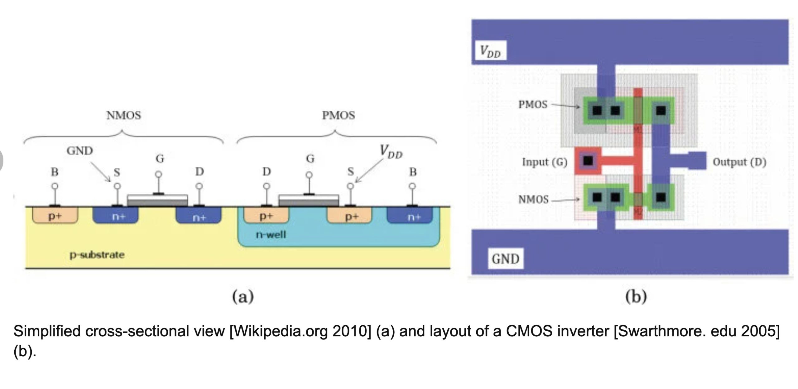
IBM Research has spent years pioneering vertical monolithic integration and complementary field-effect transistor (CFET) concepts at its Albany Nanotech Complex. The resulting 0.7nm Nanostack technology bypasses conventional 2D limitations by stacking active transistor layers directly on top of one another. By vertically integrating n-type and p-type devices within a single monolithic stack, IBM has dramatically reduced footprint area while shortening interconnect wire lengths.
"We are no longer just shrinking features on a flat plane; we are building three-dimensional micro-cities at the atomic scale," noted a senior silicon architect familiar with IBM’s internal roadmap. "The release of these design kits in Q1 2027 gives fabless innovators the foundational tools to design accelerators that achieve unprecedented transistor densities without melting under their own workloads."
This architectural leap directly addresses the primary pain point of modern AI accelerators: memory bandwidth and interconnect latency. By shrinking the physical distance electrons must travel between compute and memory cells, the Nanostack process slashes dynamic power consumption—a critical metric for enterprise data center operators striving to lower total cost of ownership (TCO) and meet stringent corporate sustainability mandates.
Market Dynamics and Financial Implications
The commercialization timeline announced for Q1 2027 carries profound valuation and risk mitigation implications across the global technology supply chain. As semiconductor fabrication plants (fabs) require billions of dollars in upfront capital expenditure (CapEx), design teams cannot afford to gamble on unproven process nodes. By shipping early Design Kits well in advance of volume production, IBM is providing system-on-chip (SoC) architects the runway necessary to optimize their intellectual property (IP) blocks for vertical scaling.
| Metric / Parameter | Legacy GAA (2nm / 3nm Class) | IBM 0.7nm Nanostack Process | Strategic Impact |
|---|---|---|---|
| Process Design Kit (PDK) Availability | Currently Market-Active | Q1 2027 (External Designers) | Enables early ecosystem validation and IP porting. |
| Transistor Architecture | Horizontal Nanosheet (GAA) | Vertical Monolithic / CFET-class Stacking | Maximizes wafer area utilization and reduces $RC$ delays. |
| Primary AI Performance Metric | High power draw at peak FLOPs | Substantial thermal and energy efficiency gains | Directly mitigates data center grid capacity constraints. |
| Target Market Segment | General Consumer / Early AI Hyperscale | Next-Gen Hyperscale AI Accelerators & Edge AI | Redefines valuation multiples for high-performance silicon providers. |
Financial analysts tracking high-eCPM and high-value enterprise tech segments point out that semiconductor manufacturing innovations of this caliber directly influence market liquidity and venture capital deployment. Companies capable of designing hardware around IBM’s Nanostack paradigm will likely command pricing power in enterprise procurement auctions, as data center operators desperately seek relief from escalating electricity bills.
Furthermore, regulatory compliance and geopolitical supply chain dynamics play a subtle yet vital role. With governments across North America and Europe subsidizing domestic semiconductor ecosystems to reduce reliance on single-region manufacturing hubs, IBM’s collaborative research model ensures that western allies retain leadership in foundational nano-architecture.
Industry & Market Implications: Winners and Losers
Every major technological paradigm shift creates clear beneficiaries and stranded assets. The democratization of the 0.7nm Nanostack process alters the competitive landscape across several key verticals:
- The Winners — Hyperscale Cloud Providers & AI Chip Innovators: Fabless startups and established cloud giants (such as Amazon, Microsoft, and Google) developing proprietary custom silicon will gain access to tools that drastically shrink die sizes. Smaller dies translate directly to higher wafer yields, lower manufacturing costs per chip, and superior performance margins.
- The Winners — Advanced Packaging & Equipment Makers: Companies specializing in extreme ultraviolet (EUV) lithography, atomic layer deposition (ALD), and 3D wafer-level bonding equipment stand to capture significant contract orders as foundries tool up to support Nanostack production lines.
- The Pressured — Traditional 2D Foundry Laggards: Foundries failing to transition rapidly past conventional horizontal nanosheet designs risk finding their portfolios commoditized as enterprise clients demand the superior energy efficiency inherent to vertical monolithic stacking.
- The Enterprise End-User: Corporate buyers deploying LLMs and autonomous enterprise software will benefit from accelerated model training times, reduced inference latency, and lower total cost of ownership as data center operators pass down energy savings.
Frequently Asked Questions (People Also Ask)
What is IBM’s 0.7nm Nanostack process, and how does it differ from traditional 2nm chips?
While standard 2nm and 3nm chips utilize horizontal gate-all-around (GAA) nanosheet transistors laid out flat across a 2D plane, IBM’s 0.7nm Nanostack process employs advanced vertical monolithic integration. By stacking active n-type and p-type transistor layers directly on top of each other, the process achieves vastly superior transistor density and shorter electrical interconnects, drastically cutting energy waste and physical die footprint.
When will chip designers gain access to the 0.7nm Nanostack technology?
IBM has confirmed that it will officially open the 0.7nm Nanostack process to external chip designers in the first quarter of 2027. This release will be accompanied by initial Process Design Kits (PDKs), allowing engineering teams to begin porting IP blocks and simulating ultra-dense architectural layouts ahead of volume manufacturing.
Why is this technological breakthrough particularly important for artificial intelligence workloads?
Generative AI and large language models require massive parallel compute capabilities that currently push data center electrical grids and thermal cooling systems to their limits. By delivering high-density performance with substantially reduced dynamic power consumption, the 0.7nm Nanostack process helps solve the thermal wall facing modern hyperscale AI accelerators, directly improving enterprise ROI and infrastructure scalability.
How does this impact the competitive dynamics among major global foundries?
By licensing or collaborating on foundational research tied to vertical stacking and CFET-class architectures, ecosystem participants gain a strategic edge over foundries reliant solely on incremental horizontal scaling. It reinforces Western semiconductor research leadership and diversifies the technological pathways available to fabless designers.
Future Outlook: Milestones to Watch Through 2027
As the industry counts down to the Q1 2027 PDK release, market analysts and research editors will monitor several crucial operational milestones. First, observe how early adopter design partners report initial simulation results regarding thermal dissipation and $RC$ delay reductions under heavy inference workloads. Second, track foundry partnership announcements, as IBM’s research breakthroughs must be successfully transitioned into high-volume manufacturing (HVM) lines at scale to achieve broad market penetration.
Ultimately, IBM’s 0.7nm Nanostack process represents a masterclass in long-term R&D capitalization. By tackling the fundamental physical limitations of silicon head-on, Big Blue is providing the architectural foundation for the next decade of artificial intelligence advancement. For enterprise leaders and capital allocators alike, positioning portfolios and technology stacks around this vertical revolution will be paramount as 2027 approaches.