Silicon Sovereignty: Inside India’s $15 Billion Bet to Upend the Global Microchip Supply Chain
NEW DELHI & MUMBAI — For decades, the global semiconductor architecture has rested on a fragile, highly concentrated axis spanning Taiwan, South Korea, and the United States. Today, a tectonic shift is underway across the sub-continent. Fueled by aggressive state intervention, billions in foreign direct investment (FDI), and a desperate global corporate hunger for supply chain de-risking, India is executing the most ambitious industrial pivot since its 1991 economic liberalization. This investigative report examines the mechanics, major players, capital allocation strategies, and geopolitical risks defining India’s semiconductor investment boom.
Executive Takeaways
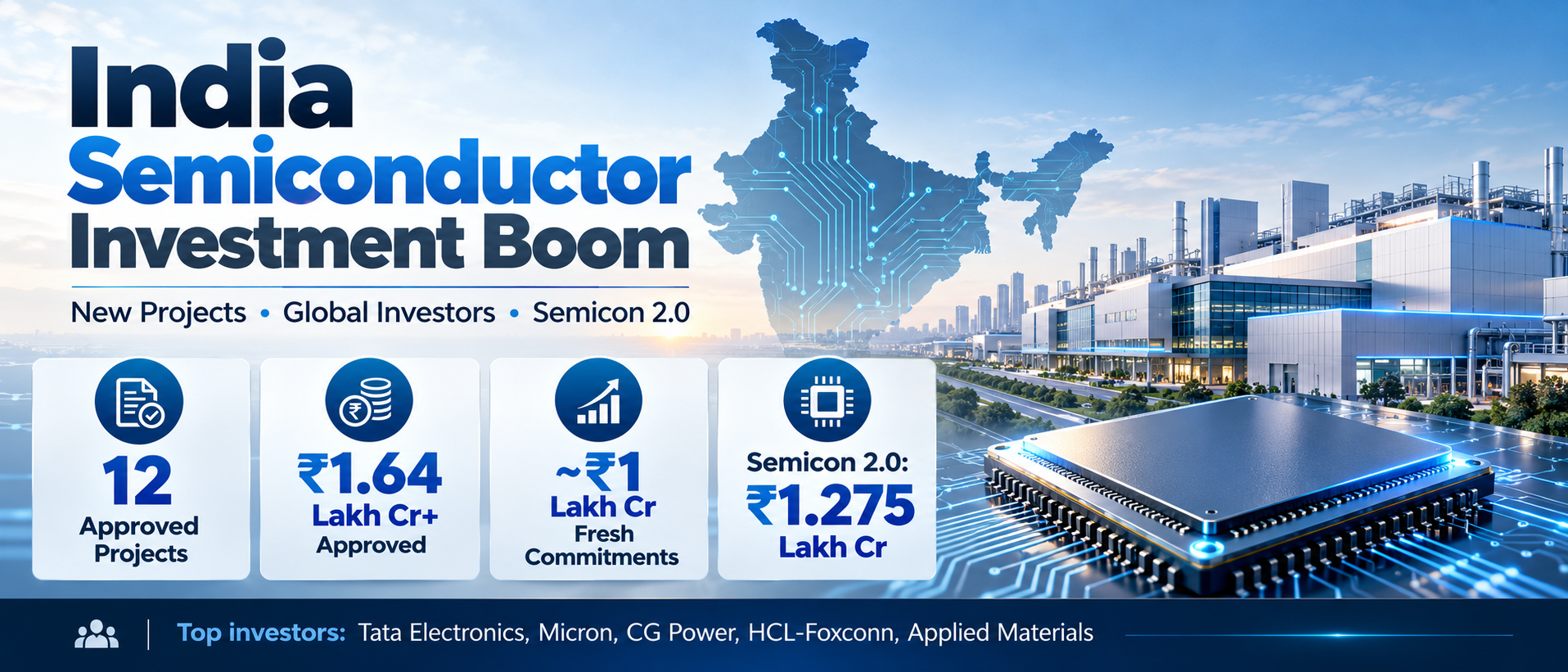
- Massive State Capital Deployment: The Indian central government has committed a $10 billion incentive outlay under the Modified Semiconductor Programme, driving total planned private and public investments past $15.2 billion across four major fabrication and assembly (OSAT) units.
- Strategic Global Partnerships: Heavyweight industrial players, including Taiwan’s PSMC, Japan’s Renesas, and U.S.-based Micron Technology, have established joint ventures and operational footprints, marking a departure from pure software outsourcing to heavy hardware manufacturing.
- Infrastructure Scalability & Risk Mitigation: While land acquisition, ultra-pure water access, and uninterrupted power grids present initial hurdles, developers are leveraging special economic zones (SEZs) and state-level regulatory compliance fast-tracking to accelerate time-to-market.
- Enterprise ROI & Market Liquidity: For institutional investors and private equity firms, the current valuation multiples in India’s deep-tech and hardware manufacturing sector signal a generational opportunity, provided execution risks are systematically mitigated.
The Catalytic Shift: Moving Beyond Code to Core Silicon
For over thirty years, India dominated the global technology landscape as the back office of the digital world. Indian engineering talent wrote the enterprise software, managed cloud compute architectures, and optimized complex algorithms for Silicon Valley giants. Yet, the physical manifestation of computing power—the semiconductor—remained entirely imported. The COVID-19 pandemic exposed the fatal vulnerabilities of this dependency, paralyzing automotive assembly lines, consumer electronics supply chains, and industrial automation globally.
Recognizing this structural vulnerability, New Delhi launched a comprehensive industrial policy overhaul designed to capture high-value manufacturing segments. The core strategy hinges on moving up the value chain from design to fabrication, packaging, and testing. By offering fiscal support covering up to 50% of project costs for semiconductor fabs, the Ministry of Electronics and Information Technology (MeitY) has transformed India from an outsider into a formidable destination for capital expenditure.
Industry veterans note that the timing aligns with a broader macroeconomic imperative. As geopolitical friction across the Taiwan Strait intensifies, multinational corporations are aggressively pursuing "China Plus One" strategies. India’s vast domestic market—booming in smartphone penetration, automotive electronics, and data center infrastructure—provides a captive consumer base that few global chipmakers can afford to ignore.
Key Projects and Global Heavyweights on the Ground

The semiconductor boom is no longer restricted to policy whitepapers; it is materializing in concrete, steel, and cleanrooms across Gujarat, Assam, and Karnataka. The projects currently underway represent a diverse cross-section of the global chip ecosystem:
- Micron Technology’s Sanand Facility (Gujarat): Representing an initial investment of $2.75 billion, Micron’s assembly, testing, marking, and packaging (ATMP) facility is the frontrunner of India’s semiconductor push. Designed to package dynamic random-access memory (DRAM) and NAND flash products, the plant highlights how rapidly global firms can deploy capital when backed by streamlined regulatory compliance.
- Tata Electronics and PSMC Partnership (Dholera, Gujarat): In one of the most significant announcements, the Tata Group has partnered with Taiwan’s Powerchip Semiconductor Manufacturing Corp (PSMC) to build India’s first commercial semiconductor fabrication plant. With an outlay exceeding $11 billion, the Dholera fab will target mature nodes (28nm, 40nm, 55nm, and 90nm) crucial for automotive, power management, and consumer electronics applications.
- CG Power, Renesas, and Stars Microelectronics (Sanand, Gujarat): A tripartite venture combining India’s Murugappa Group, Japan’s Renesas Electronics, and Thailand’s Stars Microelectronics is constructing an OSAT facility with an investment of roughly $915 million, focusing on legacy and high-growth analog chips.
- Tata OSAT Facility (Jagiroad, Assam): Adding geographical diversity to the ecosystem, Tata is investing $3.2 billion in a greenfield semiconductor assembly and test facility in Northeast India, unlocking localized manufacturing incentives and tapping into regional talent pools.
Verified Data: India Semiconductor Ecosystem Metrics
To evaluate the scale, financial commitments, and technological scope of India's nascent semiconductor landscape, consider the following verified macro-data and project breakdowns:
| Project / Venture | Global Technology Partner | Location | Estimated Capex | Target Technology / Output |
|---|---|---|---|---|
| Micron ATMP | Micron Technology (USA) | Sanand, Gujarat | $2.75 Billion | DRAM & NAND Packaging / Testing |
| Tata-PSMC Fab | PSMC (Taiwan) | Dholera, Gujarat | $11.0 Billion | 28nm - 90nm Logic Foundry |
| CG Power OSAT | Renesas (Japan) / Stars Micro | Sanand, Gujarat | $915 Million | Legacy & Analog Semiconductors |
| Tata Assam OSAT | Independent / Proprietary Tech | Jagiroad, Assam | $3.2 Billion | Advanced Packaging & Testing |
Industry & Market Implications: Winners, Losers, and Economic Realities
The systemic ripple effects of India’s semiconductor push will reshape industrial portfolios across the globe. Institutional capital allocation strategies are shifting rapidly as investors calculate enterprise ROI in an asset class traditionally viewed as too capital-intensive and cyclical for emerging markets.
The Winners
Domestic industrial conglomerates with deep balance sheets, such as the Tata Group, are positioned to capture dominant market shares in hardware manufacturing. Concurrently, specialized chemical, gas, and industrial equipment suppliers are scaling operations to feed the immense material demands of fabrication cleanrooms. Real estate developers specializing in industrial parks and high-tech warehousing near Gujarat and Karnataka are experiencing surging valuation multiples.
The Structural Bottlenecks and Potential Losers
Despite the optimism, significant friction points remain. Semiconductor manufacturing is ruthlessly unforgiving regarding infrastructure. Water and power demands are astronomical; a single advanced fab consumes millions of gallons of ultra-pure water daily and demands uninterrupted, zero-fluctuation power grids. Regions lacking these baseline utilities risk project delays. Furthermore, incumbent manufacturing hubs in Southeast Asia and East Asia face long-term competitive erosion as India systematically absorbs orders that would have previously gone to Taiwan, Malaysia, or Vietnam.
Frequently Asked Questions (People Also Ask)
1. What is the total financial commitment of India’s semiconductor incentive program?
The central government initially allocated a baseline financial outlay of $10 billion (INR 76,000 crore) specifically for the development of semiconductor and display manufacturing ecosystems. When combined with state-level subsidies from manufacturing powerhouses like Gujarat, Odisha, and Tamil Nadu, alongside private sector matching capital, total committed investments across approved projects have surpassed $15.2 billion, with further tranches expected.
2. Why are most Indian semiconductor projects focusing on mature nodes rather than cutting-edge 2nm or 3nm chips?
Mature nodes—ranging from 28nm to 90nm—drive the vast majority of the global automotive industry, industrial automation, medical devices, power management systems, and consumer appliances. By targeting mature and legacy nodes, Indian ventures can build immediate commercial viability, secure high-volume anchor customers, and master the intricate physics of wafer fabrication before attempting ultra-advanced sub-nanometer nodes.
3. How is India addressing the severe shortage of specialized semiconductor engineering talent?
Recognizing that chip design and fabrication require elite metallurgical, chemical, and microelectronic expertise, the Indian government has partnered with over 100 premier academic institutions—including the Indian Institutes of Technology (IITs)—to roll out specialized curriculum tracks. Additionally, global partners like Micron and Synopsys are establishing training centers to upskill local engineers directly on industry-standard electronic design automation (EDA) tools.
4. What are the primary risk mitigation strategies for foreign investors entering the Indian market?
Foreign investors are heavily utilizing joint-venture structures with established domestic conglomerates (such as Tata and Murugappa) to navigate regulatory compliance, land acquisition hurdles, and local stakeholder management. Furthermore, robust fiscal backing from state governments significantly cushions initial capital expenditure downside, enhancing long-term project liquidity.
Future Outlook: Milestones and the Road Ahead
The transition from policy announcements to commercial silicon output is entering its most critical phase. Over the next 24 to 36 months, financial analysts and industry observers will monitor several decisive milestones:
- First Silicon Rollout: Micron’s Sanand ATMP facility is slated to deliver its first commercially packaged chips, serving as a litmus test for Indian manufacturing efficiency.
- Construction Progression at Dholera: The physical ground-breaking and cleanroom installation at the Tata-PSMC fab will indicate whether complex foundational supply chains can be localized on schedule.
- Upstream Ecosystem Maturation: The attraction of tier-2 and tier-3 chemical, gas, and silicon wafer suppliers to domestic industrial clusters will determine whether India can achieve true self-sustaining manufacturing density rather than remaining purely an assembly outpost.
For global investors, corporate strategists, and institutional allocators, India’s semiconductor boom is no longer a speculative frontier. It is a structural reality rewriting the maps of global technology supply chains. Those who position capital intelligently within this window will capture the foundational growth of the world's next great hardware superpower.