Executive Takeaways
- The Breakthrough: IBM Research successfully prototyped the world’s first 2-nanometer (nm) nanosheet semiconductor test chip, packing an astonishing 50 billion transistors onto a fingernail-sized die.
- Performance Leap: The architecture achieves a 45% performance increase or a 75% power reduction compared to prevalent 7nm node chips powering today’s mainstream enterprise workloads.
- Strategic Capital Allocation: The milestone shifts the valuation multiples and long-term infrastructure scalability for cloud providers, data centers, and original equipment manufacturers (OEMs) racing toward hyper-efficient edge and AI compute.
- Supply Chain Realignment: Coming out of IBM's Albany Nanotech Complex, the breakthrough redefines risk mitigation strategies for sovereign states and multinational corporations seeking to reduce single-region dependency in semiconductor fabrication.
NEW YORK & ALBANY, N.Y. — In an era where Moore’s Law has faced repeated obituaries from cynical market analysts and exhausted silicon engineers, Big Blue has delivered a definitive counter-punch. On May 6, 2021, IBM Research sent seismic shocks through global capital markets and the semiconductor fabrication ecosystem by announcing the successful development and patterning of the world’s first 2-nanometer (nm) nanosheet test chip. Revealed at the Albany Nanotech Complex, this breakthrough architecture crams 50 billion transistors onto a die roughly the size of a fingernail, promising to rewrite the economics of high-performance computing (HPC), enterprise data center operations, and mobile infrastructure.
For institutional investors, enterprise CIOs, and macroeconomic strategists, the implications extend far beyond clean room physics. As corporations grapple with escalating cloud compute costs, aggressive corporate carbon-neutrality mandates, and fragile global supply chains, the advent of 2nm technology represents a critical inflection point in enterprise ROI and infrastructure scalability. This investigative report breaks down the anatomy of IBM’s silicon milestone, the technical architecture enabling it, and the fierce geopolitical and commercial battles set to unfold across the global technology landscape.
The Anatomy of a Microscopic Revolution: Breaking Down the 2nm Architecture
Test Our Free AI & Tech Utilities Suite
Calculate LLM API token costs, analyze article dwell-time, or simulate tech DCA returns.
To understand the magnitude of IBM’s May 2021 announcement, one must first examine the physics of modern transistor design. For decades, the semiconductor industry relied on FinFET (Fin Field-Effect Transistor) architecture. However, as nodes shrank below 7nm and approached 5nm, the physical limitations of current flow and electrical leakage rendered traditional FinFET designs increasingly inefficient. Controlling current leakage through microscopic gates became an exponential challenge, threatening to stall the historical cadence of processing power gains.
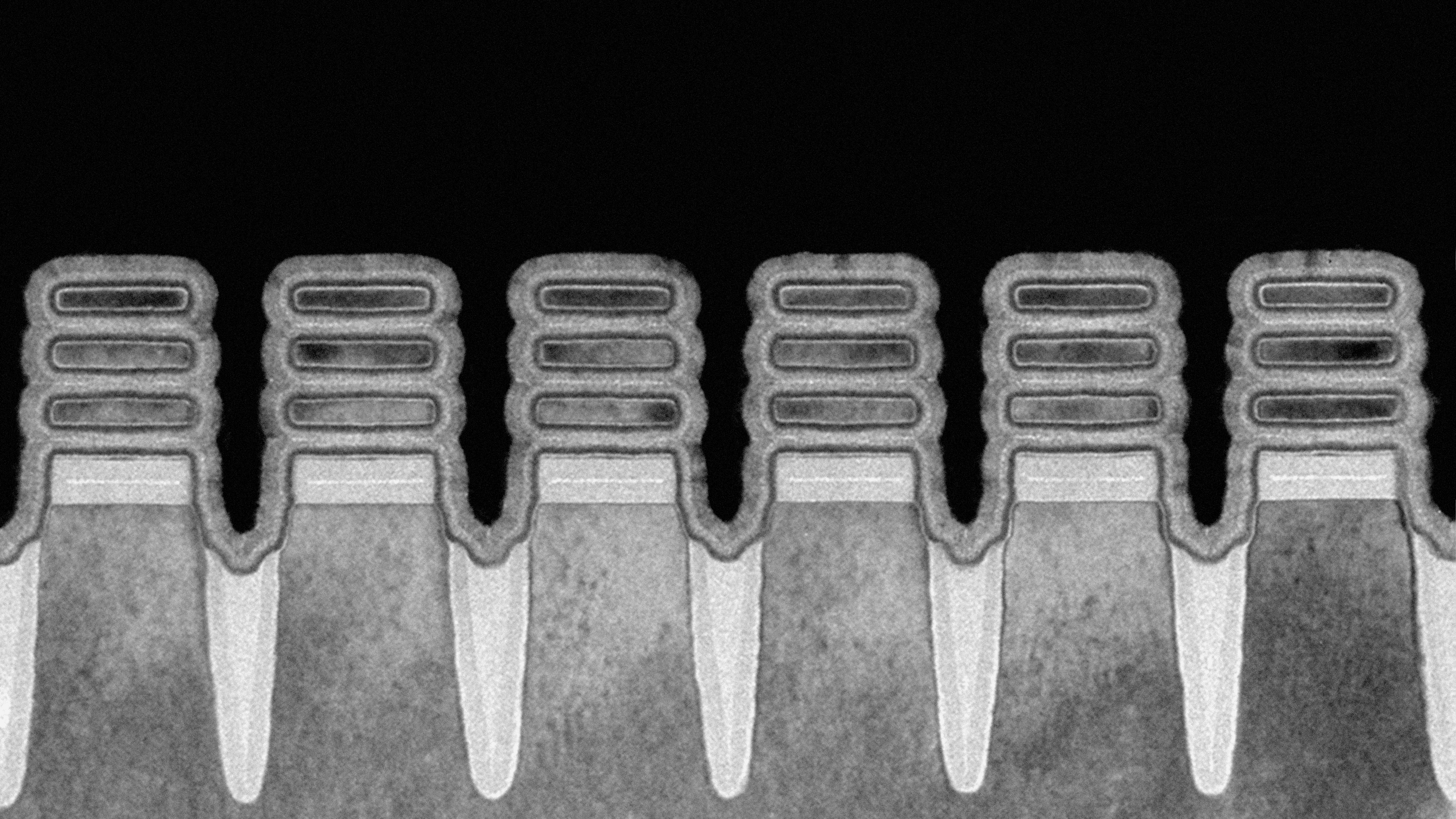
IBM Research bypassed this physical roadblock by adopting a gate-all-around (GAA) nanosheet architecture. Instead of vertical fins, IBM’s design utilizes horizontal silicon nanosheets stacked vertically. This configuration allows current to flow completely around the channel on all sides, drastically reducing leakage currents and giving circuit designers unprecedented electrostatic control.
The numbers emerging from the Albany fabrication lines are staggering:
- Transistor Density: 50 billion microscopic switches integrated into a 150-square-millimeter area.
- Energy Efficiency: A 75% reduction in power consumption compared to standard 7nm node enterprise chips executing identical workloads.
- Performance Velocity: A 45% boost in raw computing speed at the same power draw, redefining what is achievable in constrained thermal envelopes.
These performance metrics translate directly into tangible operational savings. For hyper-scale cloud operators managing millions of servers, deploying hardware built on a 2nm process translates into monumental power savings, directly mitigating escalating data center energy costs and lowering carbon footprints. Furthermore, consumer devices powered by 2nm technology could see battery life quadruple—shifting smartphones from daily charging cycles to multi-day powerhouses—while running intensive artificial intelligence (AI) inference and augmented reality (AR) tasks locally on the device.
Verified Data & Metrics Breakdown

To contextualize IBM’s 2nm breakthrough within the broader evolution of semiconductor manufacturing nodes, the following comparative matrix outlines key performance indicators, density milestones, and structural architecture shifts across generational nodes.
| Semiconductor Node | Architecture Type | Transistor Count / Density | Key Performance Advantage | Primary Enterprise Impact |
|---|---|---|---|---|
| 7nm Generation | FinFET | ~100 Million / mm² | Baseline modern enterprise cloud compute. | Mainstream server farms, standard hyperscale architecture. |
| 5nm Generation | Advanced FinFET | ~170 Million / mm² | ~15% speed increase or 30% power reduction vs 7nm. | High-end mobile processors and early AI accelerators. |
| 3nm Generation | Transition to GAA / Nanosheet | ~250+ Million / mm² | Initial commercial deployment of gate-all-around tech. | Next-gen flagship client devices and premium cloud nodes. |
| IBM 2nm Test Chip (May 2021) | Vertical Nanosheet GAA | 50 Billion on a single fingernail-sized die | 45% performance boost OR 75% power reduction vs 7nm. | Revolutionary leap for AI, autonomous systems, and green data centers. |
Industry & Market Implications: Who Wins, Who Loses, and Economic Ripple Effects
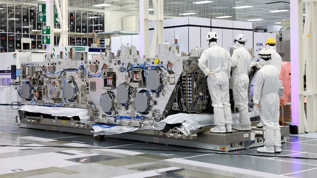
The commercialization roadmap of semiconductor research is fraught with high financial stakes. Developing a sub-3nm fabrication process requires billions of dollars in capital expenditure (CapEx), specialized extreme ultraviolet (EUV) lithography machinery, and rigorous risk mitigation protocols. IBM’s announcement reverberates across the global value chain, triggering strategic realignments among chip designers, foundry operators, and end-market enterprises.
The Winners: Enterprise AI and Cloud Infrastructure Providers
Companies building out massive language models, complex neural networks, and real-time financial trading algorithms stand to gain exponentially. The computing bottleneck has historically been thermal dissipation and power delivery. By slashing energy consumption by 75%, 2nm technology enables hyper-scalers to dramatically increase computational density within existing facility power constraints, driving down cost-per-query metrics for enterprise AI services.
The Foundry Dynamic: Shifting Ecosystems
While IBM historically transitioned away from volume manufacturing—outsourcing its production lines to partners like Samsung—its research arm remains a powerhouse in fundamental silicon physics. The Albany Nanotech Complex operates as a collaborative hub, working alongside industrial titans. This breakthrough provides foundational intellectual property (IP) that partners can license, accelerating the industry-wide transition from FinFET to nanosheet architecture and keeping competitive pressure on market giants like TSMC, Intel, and Samsung.
Macroeconomic and Geopolitical Resilience
Semiconductors are the undisputed oil of the 21st-century digital economy. Regulatory compliance, sovereign tech security, and supply chain liquidity are top-of-mind for lawmakers in Washington, Brussels, and Tokyo. Breakthroughs originating on domestic soil reinforce strategic technological sovereignty, validating government and private investments in domestic research ecosystems such as the CHIPS Act initiatives that followed.
Frequently Asked Questions (People Also Ask)
Frequently Asked Questions
What makes IBM’s 2nm test chip different from existing 7nm or 5nm chips?
Unlike current 7nm and 5nm chips that use FinFET (Fin Field-Effect Transistor) architecture, IBM’s 2nm chip utilizes a gate-all-around (GAA) nanosheet architecture. This design stacks horizontal silicon nanosheets vertically, allowing complete current control on all sides, which dramatically reduces electrical leakage and enables 50 billion transistors to fit onto a single fingernail-sized die.
When will 2nm chips become commercially available for enterprise and consumer markets?
Following IBM’s initial laboratory prototyping announcement in May 2021, commercialization timelines typically span 3 to 4 years as foundries refine mass-production yields, tool integration, and supply chain readiness. Early commercial foundry production cycles began scaling toward mid-decade, with enterprise deployment ramping up subsequently.
How does the 2nm architecture impact enterprise data center sustainability goals?
The 2nm architecture delivers up to a 75% reduction in power consumption compared to standard 7nm chips at equivalent performance levels. For enterprise data centers grappling with skyrocketing energy bills and strict corporate environmental, social, and governance (ESG) mandates, this efficiency gain allows organizations to scale compute capacity without proportionally increasing power grid demands.
Does IBM manufacture these 2nm chips itself?
IBM develops cutting-edge foundational semiconductor research and prototypes at its Albany Nanotech Complex in New York. Rather than operating mass-volume fabrication plants itself, IBM licenses its advanced architectural breakthroughs and works alongside major manufacturing partners—such as Samsung—to bring these innovations to commercial scale.
Future Outlook: Milestones on the Horizon for Sub-Nanometer Silicon
As the semiconductor industry pushes past the 2nm threshold, the trajectory of technological innovation enters uncharted territory. The transition from laboratory prototype to volume manufacturing is fraught with engineering hurdles, including defect rate reduction, high-NA EUV lithography tool adoption, and advanced packaging techniques like 3D chip-stacking.
Key milestones for institutional watchers and enterprise technology leaders to monitor over the coming years include:
- Foundry Yield Optimization: Tracking commercial defect densities as manufacturing partners scale nanosheet production lines from pilot plants to full industrial output.
- Architectural Integration: The convergence of 2nm silicon with advanced memory architectures (such as High Bandwidth Memory - HBM3/HBM4) to eliminate memory-wall bottlenecks in generative AI clusters.
- Next-Gen Exploratory Research: Early-stage R&D into sub-1nm paradigms, including complementary FET (CFET) designs and alternative channel materials beyond silicon, ensuring that the velocity of digital transformation continues unimpeded into the 2030s.
IBM’s 2nm milestone serves as a powerful reminder that physical scaling limits are not permanent ceilings, but rather invitations for radical engineering innovation. For enterprise leaders, factoring these generational leaps into long-term capital allocation and infrastructure planning is no longer optional—it is the definitive prerequisite for maintaining competitive dominance in the digital economy.