Executive Takeaways
- Unprecedented Density: IBM Research successfully prototyped the world’s first 2-nanometer (nm) nanosheet semiconductor test chip, packing 50 billion transistors onto a space the size of a fingernail.
- Performance & Efficiency Leap: The 2nm architecture delivers a 45% increase in performance or a 75% reduction in energy consumption compared to mainstream 7nm enterprise nodes.
- Macroeconomic & Capital Shifts: Arriving at a critical juncture of global supply chain vulnerabilities, this breakthrough directly influences capital allocation strategies, enterprise ROI projections, and valuation multiples across the semiconductor value chain.
- Strategic Enterprise Impact: The architecture promises transformative upgrades for mission-critical cloud compute infrastructure, artificial intelligence workloads, edge computing, and battery life extension in mobile hardware.
NEW YORK — In a milestone that fundamentally redefines the physical and economic limits of silicon engineering, IBM Research unveiled the world’s first 2-nanometer (nm) nanosheet semiconductor test chip. Announced on May 6, 2021, this landmark achievement crams an astonishing 50 billion transistors onto a die no larger than a fingernail—roughly 150 square millimeters. For enterprise technology leaders, institutional investors, and global supply chain strategists, this development is far more than a laboratory curiosity; it represents a seismic shift in infrastructure scalability, power efficiency, and long-term risk mitigation as the industry accelerates past the twilight of traditional Moore’s Law scaling.
The Catalytic Engineering Breakthrough Behind the 2nm Node
Test Our Free AI & Tech Utilities Suite
Calculate LLM API token costs, analyze article dwell-time, or simulate tech DCA returns.
For decades, the semiconductor industry has marched forward by shrinking transistor dimensions, allowing chip designers to pack more processing power into tighter spaces. However, as geometries approached the single-digit nanometer threshold, quantum mechanical effects—most notably electron leakage and severe short-channel degradation—threatened to halt progress entirely. Traditional FinFET (Fin Field-Effect Transistor) architectures, which served as the workhorse of the industry through the 14nm, 10nm, and 7nm eras, hit a physical wall when attempting to maintain gate control at sub-3nm scales.
IBM’s Albany Nanotech Complex bypassed this existential bottleneck by pioneering a gate-all-around (GAA) nanosheet architecture. Instead of upright fins, IBM utilized stacked horizontal silicon nanosheets wrapped completely by the gate material. This full encirclement maximizes electrostatic control over the channel, virtually eliminating current leakage and allowing electrons to flow with unprecedented freedom.
The numbers tell a staggering story of engineering execution. By packing 50 billion transistors into a fingernail-sized footprint, IBM achieved a transistor density of approximately 333 million transistors per square millimeter. According to benchmark validation data released by IBM Research, this architecture yields two distinct operational vectors:
- Performance Mode: A 45% boost in computing speed while operating at the same power envelope as current commercial 7nm node chips.
- Efficiency Mode: A 73% to 75% reduction in power consumption when matching the exact performance metrics of standard 7nm enterprise processors.
Such efficiency gains translate directly into tangible operational efficiencies. In hyperscale data centers—where power consumption and thermal dissipation represent the single largest operational expenditure after real estate—deploying servers powered by 2nm architecture could slash cooling and electricity overhead by nearly three-quarters. For mobile hardware, it promises smartphones that maintain full computational capability for up to four days on a single charge, fundamentally altering consumer hardware replacement cycles and ecosystem valuations.
Verified Data & Metrics Breakdown
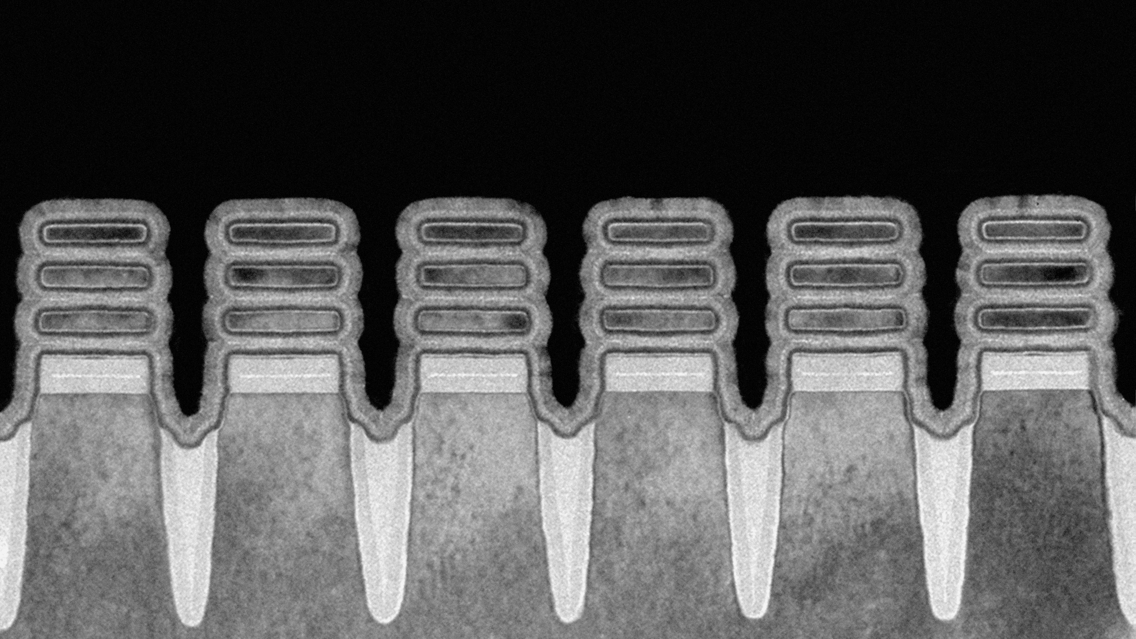
To contextualize the architectural leap represented by IBM’s 2nm test chip, the following comparative matrix outlines key engineering parameters across successive generations of semiconductor fabrication technology:
| Node Generation | Transistor Architecture | Approximate Transistor Count | Performance vs. Baseline | Power Reduction vs. Baseline |
|---|---|---|---|---|
| 7nm (Mainstream) | FinFET | ~10 to 30 Billion (per die) | Baseline (0%) | Baseline (0%) |
| 5nm (Advanced Commercial) | FinFET / Early GAA | ~15 to 150 Billion (Die size dependent) | +15% over 7nm | ~30% over 7nm |
| 2nm (IBM Research Prototype) | Gate-All-Around (GAA) Nanosheet | 50 Billion (Standard Die) | +45% over 7nm | ~75% over 7nm |
Industry & Market Implications: Capital Allocation and Competitive Dynamics
The announcement sent immediate ripples through global financial markets and boardrooms across the technology sector. As enterprises grapple with an insatiable demand for artificial intelligence, machine learning model training, cryptographic processing, and cloud compute architecture, the underlying hardware economics dictate corporate profitability.
Winners and Losers in the Ecosystem: Foundries and equipment manufacturers capable of tooling up for extreme ultraviolet (EUV) lithography and advanced nanosheet fabrication stand to capture substantial market share. Conversely, legacy manufacturers locked into outdated FinFET nodes face compressed valuation multiples and accelerated obsolescence. For enterprise software developers, the arrival of 2nm hardware unlocks the computational headroom required to run complex, real-time generative AI models at the network edge without relying exclusively on power-hungry data center clusters.
Capital Allocation and Risk Mitigation: Transitioning from research prototyping to commercial high-volume manufacturing (HVM) requires immense capital expenditure (CapEx), often running into tens of billions of dollars per fabrication plant. Corporate treasuries are being forced to reallocate capital toward R&D partnerships, supply chain diversification, and intellectual property acquisition. In an era marked by geopolitical friction and regulatory compliance hurdles surrounding semiconductor trade, owning foundational IP like IBM’s nanosheet design provides critical risk mitigation against supply chain bottlenecks.
People Also Ask (FAQ)
What is a 2nm semiconductor chip, and why is it important?
A 2nm chip refers to a semiconductor fabricated using features measuring approximately 2 nanometers in scale. It is important because packing more transistors into a smaller area dramatically increases processing speeds while slashing energy consumption, addressing critical power and thermal limits in modern computing infrastructure.
How many transistors are on IBM’s 2nm test chip?
IBM’s 2nm test chip integrates 50 billion transistors onto a single piece of silicon roughly the size of a fingernail (approximately 150 square millimeters), translating to an unprecedented transistor density.
What makes Gate-All-Around (GAA) nanosheets superior to older FinFET designs?
Unlike traditional FinFET architectures where the gate contacts the channel on three sides, GAA nanosheets wrap the gate completely around the channel on all four sides. This provides superior electrostatic control, reduces current leakage, and enables continued scaling past the physical limits of 3nm nodes.
When will 2nm chips be available in commercial enterprise hardware?
Following IBM’s initial laboratory prototyping and architectural validation, major commercial foundries and ecosystem partners target volume manufacturing and enterprise deployment in the mid-2020s, subject to tool readiness and cleanroom capacity scaling.
Future Outlook: Milestones on the Road to Commercialization
While IBM’s announcement marks a profound scientific triumph, the journey from a functional laboratory test chip to mass-produced enterprise hardware involves overcoming formidable hurdles. Foundry partners must refine extreme ultraviolet (EUV) lithography techniques—specifically high-numerical aperture (High-NA) EUV systems—to pattern the delicate nanosheet structures with zero yield loss.
Key milestones for institutional investors and technology executives to monitor over the next 24 to 36 months include:
- PDK Release & Ecosystem Tooling: The rollout of Process Design Kits (PDKs) to fabless chip designers, enabling them to begin architectural simulation and layout design for 2nm tape-outs.
- Pilot Line Yield Stabilization: Demonstration of commercially viable defect densities and wafer yields in pilot manufacturing lines, proving that nanosheet technology can be scaled economically.
- <Hyperscaler Adoption Announcements: Strategic partnerships between pioneering foundries and major cloud providers (such as Amazon Web Services, Microsoft Azure, and Google Cloud) committing to custom silicon designs built on 2nm nodes.
Ultimately, IBM’s 2nm breakthrough signals that the death of Moore’s Law has been greatly exaggerated. By reimagining the physical geometry of the transistor at the atomic level, the semiconductor industry has secured its trajectory, ensuring that enterprise computing power will continue to scale to meet the soaring demands of the digital economy well into the next decade.