Executive Takeaways
- The Core Blueprint: India’s semiconductor industrial policy has matured past bureaucratic announcements, boasting an active 2026 portfolio anchored by 1 premier silicon wafer fabrication plant and 2 advanced compound semiconductor facilities.
- Capital Allocation & Valuations: Backed by the multi-billion-dollarModified Programme for Semiconductors and Display Ecosystem, corporate capital expenditure (CapEx) from global joint ventures is fundamentally reshaping South Asia’s hardware valuation multiples and supply chain resilience.
- Geographic Clustering: Gujarat and Assam have emerged as the primary epicenters of high-tech manufacturing, drawing massive foreign direct investment (FDI) and forcing state-level infrastructure scalability upgrades.
- Enterprise Risk & Talent Mitigation: While supply chain de-risking provides attractive long-term market liquidity, systemic bottlenecks in ultra-pure water access, uninterrupted industrial power, and specialized engineering talent remain critical variables.
NEW DELHI — For decades, the global semiconductor paradigm was anchored by a precarious geographical bottleneck: a handful of East Asian foundries producing the microscopic silicon brains that power everything from consumer smartphones to intercontinental ballistic missiles. By mid-2026, that geopolitical monopoly has fractured irrevocably. Driven by aggressive state subsidies, shifting multinational capital allocation strategies, and an urgent mandate for supply chain risk mitigation, India has transitioned from a software and services giant into a hard-tech manufacturing frontier.
As detailed in recent industry tracking, including benchmark analyses from Jagran Josh, India’s domestic silicon landscape is no longer a speculative blueprint. It is a live construction site of high-stakes enterprise bets, foreign partnerships, and complex cleanroom engineering. For institutional investors, multinational technology conglomerates, and supply chain executives, understanding the precise geographical distribution, technological specifications, and economic viability of India’s semiconductor plants is no longer optional—it is an exercise in enterprise survival.
The Catalytic Shift: Why 2026 Marks the Inflection Point
To understand the current valuation multiples and operational footprints of India’s semiconductor sector, one must examine the macro-level policy architecture that catalyzed this transformation. The Indian government’s $10 billion Semiconductor Mission, combined with lucrative state-level financial incentives, fundamentally altered the risk-reward ratio for global chipmakers. Faced with escalating geopolitical friction between Washington and Beijing, boardrooms across Silicon Valley, Taipei, and Tokyo realized that geographic diversification was a mandatory hedge against catastrophic market liquidity disruptions.
However, building a semiconductor ecosystem requires more than fiscal subsidies; it demands an intricate ecosystem of chemical suppliers, specialized gases, ultra-reliable power grids, and an immense pool of photolithography and materials science engineers. By 2026, the initial wave of approved projects has moved past the memorandum-of-understanding (MoU) phase and into active ground-level execution. The current industrial breakdown—featuring 1 primary silicon fab and 2 advanced compound semiconductor facilities—reflects a calculated strategy: capturing foundational manufacturing share while establishing specialized niches in power electronics and optoelectronics.
The 2026 Semiconductor Plant Registry: Locations and Technical Profiles
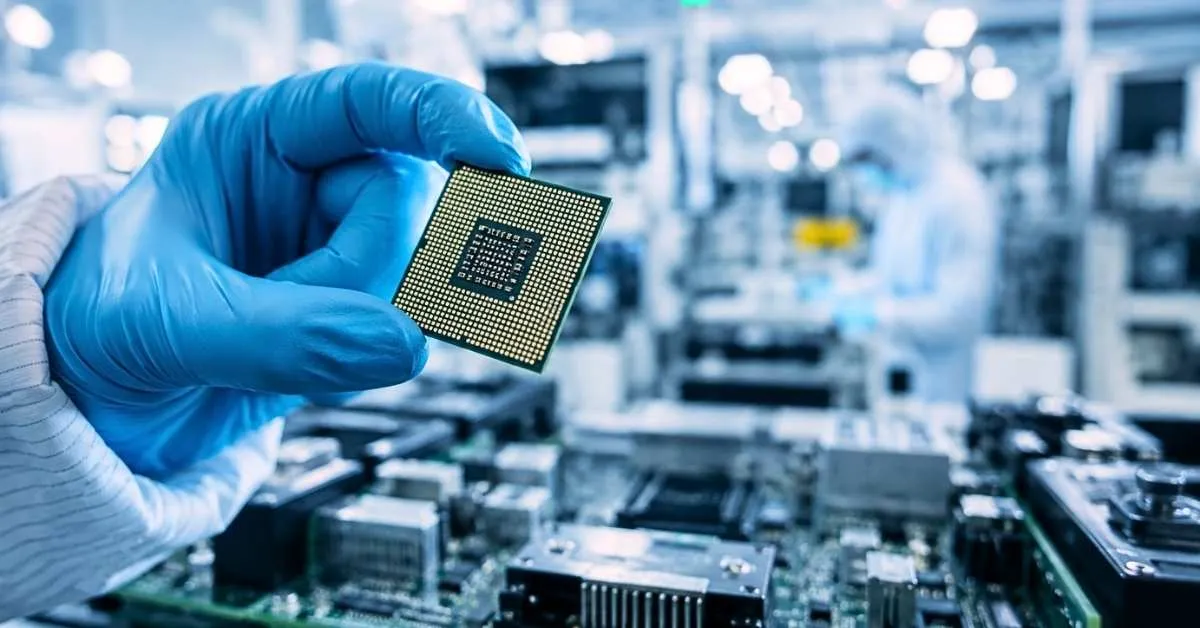
A rigorous examination of India’s semiconductor footprint reveals a deliberate clustering strategy. Rather than dispersing capital haphazardly across the subcontinent, regional authorities have concentrated infrastructural investments in states capable of scaling logistical and utilities support.
1. Gujarat’s Silicon Core: The Dholera Mega-Fab
The crown jewel of India’s silicon ambitions is located in Gujarat’s Dholera Special Investment Region. This facility represents the country's sole primary silicon wafer fabrication plant in the current commercial pipeline. Operating through a high-profile joint venture involving domestic industrial titan Tata Group and Taiwan’s Powerchip Semiconductor Manufacturing Corp (PSMC), the Dholera fab is designed to address mature and legacy nodes that form the backbone of automotive, industrial, and consumer electronics applications.
From an enterprise ROI perspective, targeting mature nodes (such as 28nm to 65nm architectures) is a masterclass in market capture. While cutting-edge 2nm and 3nm nodes capture headlines, global industrial demand for legacy chips remains insatiable. The Dholera plant leverages PSMC’s proven foundry operating system, minimizing technological execution risk while maximizing immediate commercial offtake agreements with global original equipment manufacturers (OEMs).
2. Compound Semiconductor Hubs: Gujarat and Assam
Beyond silicon, the 2026 landscape is defined by two specialized compound semiconductor facilities. Compound semiconductors—utilizing materials like Gallium Nitride (GaN) and Silicon Carbide (SiC)—are critical for high-frequency, high-voltage applications, including electric vehicle (EV) powertrains, 5G telecom infrastructure, and defense radar systems.
- Sanand, Gujarat: Home to specialized outsourced semiconductor assembly and test (OSAT) and compound semiconductor operations, notably spearheaded by partnerships such as Renesas and CG Power alongside Murata. This facility benefits immensely from Gujarat's pre-existing automotive and chemical manufacturing clusters, ensuring seamless supply chain integration.
- Jagiroad, Assam: Representing a groundbreaking geopolitical and economic push into India’s Northeast, the Tata OSAT facility in Jagiroad bridges the technological divide for the region. This plant focuses on advanced packaging, flip-chip, and wire-bonding technologies—critical steps that transform raw silicon wafers into finished, market-ready microchips. The strategic placement underscores a broader federal mandate for inclusive regional industrial development and equitable market liquidity distribution.
Verified Data Matrix: India Semiconductor Ecosystem (2026)
The following table outlines the structural composition, technological focus, and capital architecture of India's primary active semiconductor projects:
| Facility Name | Location | Technology Type | Key Partners / Promoters | Strategic Focus |
|---|---|---|---|---|
| Dholera Silicon Fab | Dholera, Gujarat | Silicon Wafer Fabrication (Mature Nodes) | Tata Electronics & PSMC (Taiwan) | Automotive, Power Management, Consumer Electronics |
| Sanand Compound Facility | Sanand, Gujarat | OSAT & Compound Semiconductors | CG Power, Renesas, & Murata | EV Powertrains, 5G Infrastructure, Industrial Power |
| Jagiroad Packaging Unit | Jagiroad, Assam | Advanced Semiconductor Packaging (OSAT) | Tata Electronics | High-Density Packaging, Flip-Chip, Export Markets |
Industry & Market Implications: Who Wins and Who Loses?
The maturation of India’s semiconductor plants in 2026 is sending shockwaves through global balance sheets, creating distinct corporate winners and losers across the hardware value chain.
The Winners
- Global Automakers and Industrial OEMs: Companies heavily reliant on microcontrollers and power management ICs now have a viable secondary sourcing hub inside the Indo-Pacific trade corridor, sharply mitigating geopolitical supply shock vulnerabilities.
- Domestic Engineering and Infrastructure Conglomerates: Firms specializing in industrial construction, water purification, heavy electrical engineering, and cleanroom design are seeing unprecedented revenue growth and margin expansion.
- Specialized Chemical and Gas Suppliers: Global specialty chemical enterprises that establish local blending and distribution channels in Gujarat and Assam are locking in long-term sticky contracts with high switching costs.
The Vulnerabilities and Loses
- Legacy East Asian Foundry Monopolies: While not facing immediate displacement at cutting-edge nodes, traditional regional players are watching their mature-node pricing power compress as Indian state-backed capacity comes online.
- Local Resource-Intensive Sectors: Semiconductor manufacturing is notoriously demanding on local utilities. Regions hosting these plants face intense scrutiny regarding water table depletion and municipal power grid stability, necessitating strict regulatory compliance and green infrastructure investments.
Frequently Asked Questions (People Also Ask)
1. How many semiconductor plants are currently operational or approved in India as of 2026?
As of mid-2026, India's active semiconductor manufacturing roster comprises a foundational breakdown of 1 primary silicon wafer fabrication plant (located in Dholera, Gujarat) and 2 major compound semiconductor and OSAT facilities (located in Sanand, Gujarat, and Jagiroad, Assam), alongside several smaller assembly and design validation outposts approved under the broader national incentive framework.
2. What is the primary technological focus of the Tata-PSMC Dholera Fab?
The Dholera plant focuses primarily on mature and legacy semiconductor nodes (ranging from 28nm to 65nm). These nodes are heavily utilized in automotive systems, power management integrated circuits (PMICs), display driver ICs, and microcontrollers, matching immediate global enterprise demand rather than bleeding-edge consumer smartphone processors.
3. Why are compound semiconductors being manufactured in places like Sanand and Assam?
Compound semiconductors utilize materials such as Silicon Carbide (SiC) and Gallium Nitride (GaN), which operate efficiently under extreme voltages and frequencies—making them indispensable for Electric Vehicle (EV) inverters, renewable energy grids, and 5G telecommunications infrastructure. Placing these plants in industrial hubs like Sanand and Assam allows operators to leverage regional logistics, automotive clusters, and state-level tax incentives.
4. What are the primary risk factors facing India’s semiconductor manufacturing push?
Despite robust capital allocation and government backing, key risks include maintaining uninterrupted ultra-pure water supplies, securing stable baseload industrial power, managing complex regulatory compliance across state lines, and closing the structural talent gap for specialized cleanroom technicians and semiconductor design engineers.
Future Outlook: Milestones and Strategic Horizon
Looking toward the remainder of the decade, India’s semiconductor trajectory will be judged not by groundbreaking ceremonies, but by commercial yield rates, wafer output volumes, and the integration of domestic chips into global supply chains. Key milestones to watch over the next 24 to 36 months include the first commercial tape-outs from the Dholera fab, the scaling of OSAT export volumes out of Assam, and potential announcements regarding secondary-node expansions into 14nm and 22nm architectures.
For institutional investors and enterprise strategists, India has successfully graduated from a conceptual semiconductor market to a tangible manufacturing reality. Navigating this landscape successfully requires continuous monitoring of utility scalability, regulatory shifts, and joint-venture execution metrics. The silicon revolution on the subcontinent is no longer a distant projection—it is actively printing the hardware of tomorrow.