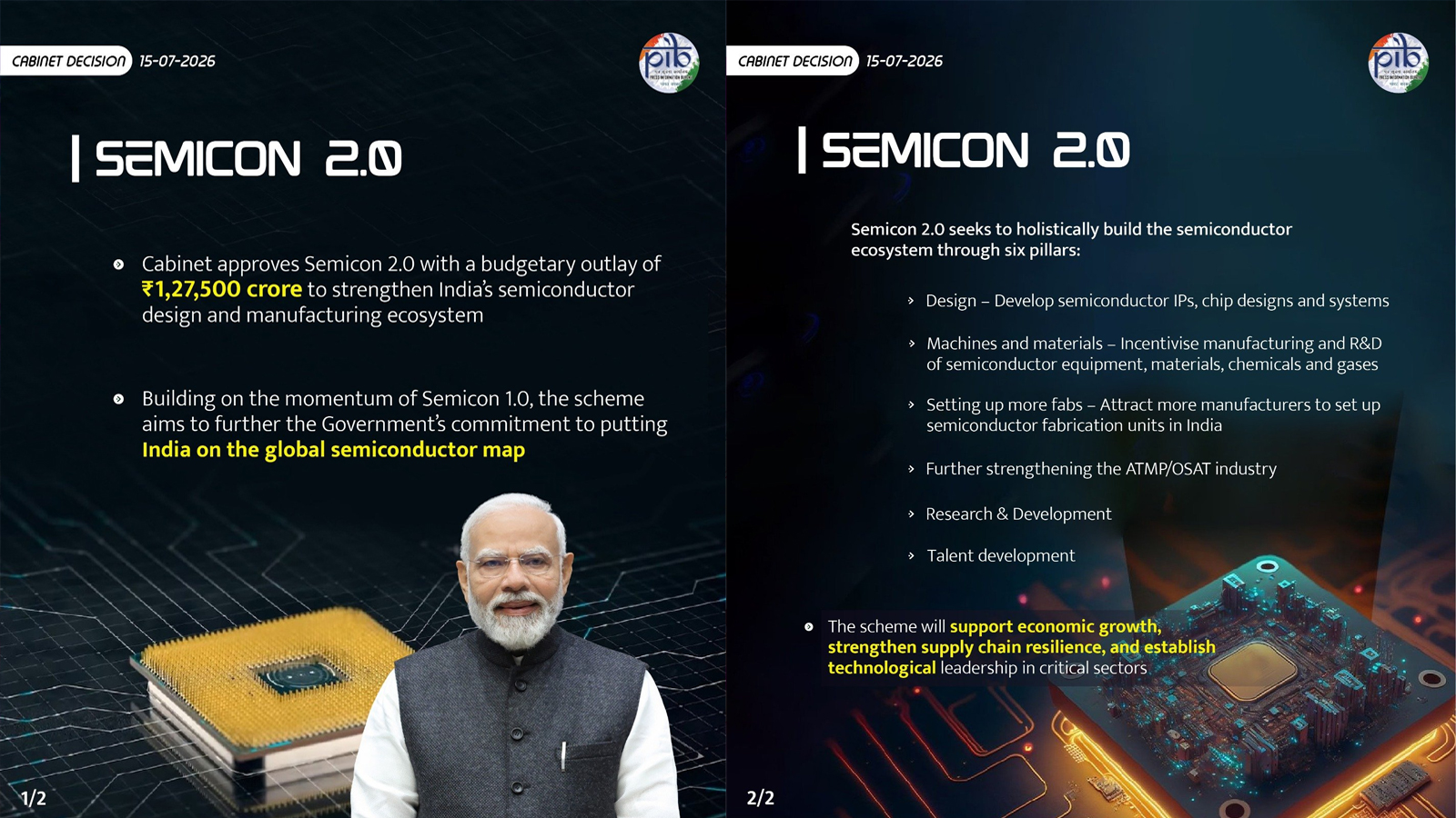
NEW DELHI — In an assertive bid to permanently realign the geopolitical geography of critical technology, the Union Cabinet has greenlit "Semicon India 2.0," authorizing a massive fiscal allocation of ₹1.27 lakh crore ($15.2 billion). The sequel to India’s initial semiconductor foray represents a radical expansion in sovereign capital allocation, aimed at transforming the subcontinent from an opportunistic packaging outpost into an end-to-end silicon powerhouse capable of challenging traditional East Asian manufacturing bastions.
According to high-level briefings following the Cabinet meeting, the revised program is engineered to act as institutional equity-style leverage, designed to catalyze at least ₹4 lakh crore ($48 billion) in cumulative gross capital formation across fabs, advanced packaging, raw substrate purification, and indigenous intellectual property (IP) design. Coming at a critical inflection point in post-pandemic supply chain restructuring and mounting cross-strait geopolitical friction, New Delhi’s mega-package establishes structural risk mitigation for global enterprise OEMs seeking resilient cloud compute architecture, automotive silicon, and telecommunications hardware.
Executive Takeaways
- Unprecedented Fiscal Injection: The Union Cabinet has approved ₹1.27 lakh crore ($15.2 billion) for the Semicon India 2.0 framework, superseding the inaugural ₹76,000 crore program launched in December 2021.
- High-Velocity Private Capital Multiplier: Government projections estimate the sovereign capital backstop will crowd-in over ₹4 lakh crore ($48 billion) in private sector capital expenditure, expanding direct electronics production capacity fourfold by 2030.
- Pivot to Upstream & Compound Silicon: While Semicon 1.0 prioritized trailing-edge logic (28nm–40nm) and traditional assembly, Version 2.0 aggressively subsidizes specialized silicon carbide (SiC) and gallium nitride (GaN) compound fabs, raw wafer manufacturing, equipment component fabrication, and domestic electronic design automation (EDA) software.
- Institutional De-Risking for Global Tech: The policy addresses systemic vulnerabilities highlighted by global enterprises, offering comprehensive infrastructure scalability, 50% flat central fiscal support on capex, and streamlined regulatory compliance regimes designed to compress industrial project gestation times.
The Genesis of Semicon 2.0: Moving Past Assembly to Deep Infrastructure
When the original Semicon India scheme launched in late 2021 with a ₹76,000 crore outlay, critics dismissed it as a late-cycle entry into a capital-intensive industry characterized by steep learning curves, brutal cyclicality, and consolidated moats held by Taiwan, South Korea, and the United States. However, the initial phase succeeded in breaking industrial inertia, landing anchor investments including the Tata Electronics-Powerchip Semiconductor Manufacturing Corp (PSMC) commercial foundry in Dholera, Micron’s advanced assembly and test facility in Sanand, and joint OSAT ventures involving CG Power, Renesas, and the Murugappa Group.
Yet, industrial audits conducted across 2024 and 2025 revealed distinct structural vulnerabilities. India’s nascent ecosystem remained critically dependent on imported raw silicon ingots, specialty gases, photochemicals, and offshore electronic design tools. Furthermore, trailing-edge logic fab economics faced margin compression, while global enterprise demand exploded for power semiconductors driving electric mobility, industrial automation, and AI-optimized data center infrastructure.
Semicon India 2.0 has been architected to eliminate these strategic chokepoints. Instead of focusing solely on commercial logic foundries, the ₹1.27 lakh crore allocation diversifies public capital across the entire supply stack:
- Raw Materials and Specialty Consumables: Up to 50% capital subsidies for chemical processing plants delivering ultra-pure electronic-grade hydrogen peroxide, silane, specialty gases, and quartzware.
- Compound Semiconductors (SiC/GaN): Targeted incentives for wide-bandgap semiconductors, securing supply chains for India’s accelerating electric vehicle (EV) sector, renewable grid inverters, and 5G/6G RF transceivers.
- Semiconductor Manufacturing Equipment Components: Direct support for Tier-2 and Tier-3 precision engineering suppliers to build localized spare-parts ecosystems for lithography, etch, and deposition tooling.
- Expanded Design-Led Incentive (DLI) Scheme: Substantial expansion of sovereign compute credits and financial underwriting for domestic fabless chip startups aiming to develop proprietary System-on-Chip (SoC) architectures.
Capital Efficiency and Enterprise ROI: The Financial Architecture
For institutional investors and multinational boardrooms evaluating capital allocation, the economics of Semicon India 2.0 provide compelling risk-adjusted returns. Modern commercial fabs operate under punishing capital expenditure profiles, where cleanroom infrastructure, extreme ultraviolet (EUV) or deep ultraviolet (DUV) lithography systems, and high-vacuum tooling consume 75% to 80% of project costs before a single commercial wafer is processed.
Under the enhanced scheme, the Central Government maintains its cornerstone offering: a uniform 50% fiscal support on capital expenditure on a pari-passu basis. Crucially, host state governments—such as Gujarat, Tamil Nadu, Karnataka, and Maharashtra—frequently supplement this with an additional 20% to 25% capex subsidy, alongside subsidized industrial land, high-voltage dual-grid power guarantees, and long-term water tariff concessions.
This dual-tiered incentive structure effectively shields global semiconductor joint ventures from early-stage burn rates. By reducing initial equity exposure by up to 70%, enterprise ROI profiles improve drastically. The blended capital cost model lowers the break-even threshold on wafer yields, allowing consortium partners to sustain competitive gross margins even during global cyclical downturns in chip spot prices.
Data Breakdown: Semicon 1.0 vs. Semicon 2.0 Policy Evolution
| Metric / Parameter | Semicon India 1.0 (2021) | Semicon India 2.0 (2026) |
|---|---|---|
| Total Outlay | ₹76,000 Crore ($9.1B) | ₹1,27,000 Crore ($15.2B) |
| Projected Private Capex Multiplier | ₹1.50 - ₹2.00 Lakh Crore | ₹4.00 Lakh Crore ($48B) |
| Primary Technological Node Focus | Trailing edge (28nm, 40nm, 65nm) logic | Compound Silicon (SiC/GaN), Memory, Advanced Packaging, Sub-28nm Roadmap |
| Supply Chain Integration | Isolated Fabs & Assembly Units | Integrated Ecosystem: Chemicals, Gases, Equipment Spares, Substrates |
| Design Support Scope | ₹1,000 Crore Cap; Limited Fabless Traction | Expanded Sovereign Cloud Compute Infrastructure, EDA Licensing Subsidies |
| Workforce Training Pipeline | Target: 85,000 Engineers across 5 years | Institutionalized R&D Clusters with Taiwan/US academic tie-ups (Target: 250,000) |
Geopolitical Realignment: The China+1 Reality in Silicon
The timing of the Union Cabinet’s approval highlights New Delhi's calculated positioning within the shifting geopolitical landscape. With Western tech giants aggressively executing supply chain redundancy strategies away from Mainland China, and with enterprise risk teams pricing in potential disruptions across the Taiwan Strait, India offers a politically neutral, highly scalable manufacturing sanctuary.
Under the US-India Initiative on Critical and Emerging Technology (iCET) and bilateral supply chain agreements with the European Union and Japan, India is actively positioning its fabs and testing facilities as trusted nodes within allied technology networks. Global hyperscalers expanding enterprise data centers across the Asia-Pacific region, alongside automotive conglomerates standardizing electric powertrain architectures, view India as a vital alternative hub for continuous, disruption-free chip supply.
Industry & Market Implications: Winners, Structural Friction, and Vulnerabilities
The Beneficiaries
- Domestic Industrial Conglomerates: Groups like Tata Electronics, Murugappa, and Vedanta gain substantial fiscal runway to scale execution capabilities, enhance technical licensing agreements with overseas foundries, and achieve favorable long-term enterprise valuation multiples.
- Global Fabless Design Houses: Companies such as Qualcomm, MediaTek, AMD, and Intel—which already maintain massive enterprise R&D workforces across Bengaluru and Hyderabad—will benefit from a localized ecosystem where prototypes can be taped out, packaged, and verified domestically.
- Automotive and Industrial Electronics Sectors: Domestic automotive Tier-1 suppliers (e.g., Bosch India, Uno Minda, Sona BLW) stand to benefit from reduced delivery lead times and minimized cross-border freight volatility for mission-critical microcontrollers and power modules.
Persistent Headwinds & Execution Risks
Despite the immense capital deployment, structural challenges remain. Semiconductor fabrication facilities consume tens of millions of liters of ultrapure water per day and require uninterrupted, transient-free electrical power. Any micro-fluctuation in grid frequency can corrupt an entire production batch of silicon wafers, generating tens of millions of dollars in scrapped inventory.
Furthermore, India faces intense competition for high-end talent. While the country supplies roughly 20% of the world’s chip design engineers, it lacks seasoned shop-floor fab operational directors, lithography process specialists, and cleanroom maintenance engineers. Addressing this deficit requires sustained institutional partnerships and rapid deployment of expatriate technical leaders to train domestic teams during the initial production ramp.
Frequently Asked Questions (People Also Ask)
What is the core difference between Semicon India 1.0 and Semicon India 2.0?
While Semicon India 1.0 (₹76,000 crore) focused on attracting baseline commercial foundries and OSAT/ATMP assembly units to initiate an ecosystem, Semicon India 2.0 (₹1.27 lakh crore) expands upstream. It aggressively funds the foundational ecosystem—including specialty manufacturing equipment components, electronic-grade chemicals, gases, silicon carbide/gallium nitride (SiC/GaN) compound semiconductors, and enterprise-grade EDA tools for domestic fabless chip developers.
How does the 50% fiscal subsidy mechanism function for global corporations?
The Government of India provides a 50% fiscal subsidy on the total project capital expenditure (capex) on an ongoing, equal-footing (pari-passu) basis. This is non-dilutive sovereign financial backing directly offsetting hardware, construction, cleanroom, and tooling expenses. In most states, state-level matching grants provide an additional 20% to 25%, drastically lowering equity barriers and de-risking long-term investment.
Why is India prioritizing compound semiconductors over sub-5nm advanced nodes?
Sub-5nm fabrication requires multi-billion-dollar Extreme Ultraviolet (EUV) lithography infrastructure, highly monopolized supply chains, and decades of institutional memory. By contrast, compound semiconductors (SiC and GaN) and mature trailing-edge logic (28nm to 65nm) represent the vast majority of real-world enterprise volume, powering electric vehicles, solar infrastructure, 5G/6G base stations, consumer appliances, and defense electronics. This strategy maximizes capital efficiency and local value creation while building institutional execution competence.
What is the timeline for India's first commercially operational semiconductor fab?
Initial commercial pilot production from early-phase facilities, such as Micron's Sanand OSAT plant and the Tata-PSMC Dholera foundry, is scheduled to initiate commercial wafer runs and packaged testing cycles between late 2025 and 2026. The full industrial output enabled by the newly sanctioned Semicon India 2.0 capital allocation is targeted to achieve commercial scale between 2027 and 2030.
The Road Ahead: Milestones to Monitor (2026–2030)
As the India Semiconductor Mission (ISM) operationalizes the ₹1.27 lakh crore package, market participants and enterprise strategists should monitor several key milestones over the coming 24 to 36 months:
- First Wafer Out and Defect Density Metrics: Initial pilot yields from the Tata-PSMC Dholera facility will provide the primary test of India's ability to maintain world-class silicon purity and operational uptime.
- Anchor Equipment Manufacturer Tie-Ups: Announcements of localized manufacturing centers by Tier-1 semiconductor tooling vendors—such as Applied Materials, Lam Research, or Tokyo Electron—will signal that India's ecosystem has achieved structural critical mass.
- Commercial Commercialization of Compound Silicon: The speed at which localized SiC and GaN fabs achieve automotive and industrial grade-qualification (AEC-Q100) will determine whether India captures the high-margin margins of the global EV revolution.
By transforming sovereign balance-sheet strength into long-term technology infrastructure, India’s Semicon 2.0 program is no longer merely an industrial subsidy scheme. It represents a structured, well-capitalized strategy to carve out an indispensable role in the 21st-century technology supply chain.